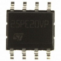
M25PE20-VMN6TP NUMONYX, M25PE20-VMN6TP Datasheet - Page 13

M25PE20-VMN6TP
Manufacturer Part Number
M25PE20-VMN6TP
Description
IC FLASH 2MBIT 75MHZ 8SOIC
Manufacturer
NUMONYX
Series
Forté™r
Datasheet
1.M25PE10-VMN6TP.pdf
(64 pages)
Specifications of M25PE20-VMN6TP
Format - Memory
FLASH
Memory Type
FLASH
Memory Size
2M (256K x 8)
Speed
75MHz
Interface
SPI, 3-Wire Serial
Voltage - Supply
2.7 V ~ 3.6 V
Operating Temperature
-40°C ~ 85°C
Package / Case
8-SOIC (3.9mm Width)
Cell Type
NOR
Density
2Mb
Access Time (max)
8ns
Interface Type
Serial (SPI)
Boot Type
Not Required
Address Bus
1b
Operating Supply Voltage (typ)
3.3V
Operating Temp Range
-40C to 85C
Package Type
SOIC N
Sync/async
Synchronous
Operating Temperature Classification
Industrial
Operating Supply Voltage (min)
2.7V
Operating Supply Voltage (max)
3.6V
Word Size
8b
Number Of Words
256K
Supply Current
8mA
Mounting
Surface Mount
Pin Count
8
Lead Free Status / RoHS Status
Lead free / RoHS Compliant
Other names
M25PE20-VMN6TPTR
Available stocks
Company
Part Number
Manufacturer
Quantity
Price
Company:
Part Number:
M25PE20-VMN6TP
Manufacturer:
MICRON
Quantity:
3 000
Company:
Part Number:
M25PE20-VMN6TP
Manufacturer:
Numonyx
Quantity:
16 500
Part Number:
M25PE20-VMN6TP
Manufacturer:
MICRON/美光
Quantity:
20 000
M25PE20, M25PE10
4.3
4.4
4.5
4.6
A fast way to modify data
The Page Program (PP) instruction provides a fast way of modifying data (up to 256
contiguous bytes at a time), provided that it only involves resetting bits to 0 that had
previously been set to 1.
This might be:
●
●
●
For optimized timings, it is recommended to use the Page Program (PP) instruction to
program all consecutive targeted bytes in a single sequence versus using several Page
Program (PP) sequences with each containing only a few bytes (see
Program
and
Polling during a Write, Program or Erase cycle
A further improvement in the write, program or erase time can be achieved by not waiting for
the worst case delay (t
provided in the Status Register so that the application program can monitor its value, polling
it to establish when the previous cycle is complete.
Reset
An internal power-on Reset circuit helps protect against inadvertent data writes. Addition
protection is provided by driving Reset (Reset) Low during the power-on process, and only
driving it High when V
Active Power, Standby Power and Deep Power-down modes
When Chip Select (S) is Low, the device is selected, and in the Active Power mode.
When Chip Select (S) is High, the device is deselected, but could remain in the Active Power
mode until all internal cycles have completed (Program, Erase, Write). The device then goes
in to the Standby Power mode. The device consumption drops to I
The Deep Power-down mode is entered when the specific instruction (the Deep Power-
down (DP) instruction) is executed. The device consumption drops further to I
device remains in this mode until the Release from Deep Power-down instruction is
executed.
Table 24: AC characteristics (75 MHz operation, T9HX (0.11 µm)
when the designer is programming the device for the first time
when the designer knows that the page has already been erased by an earlier Page
Erase (PE), SubSector Erase (SSE), Sector Erase (SE) or Bulk Erase (BE) instruction.
This is useful, for example, when storing a fast stream of data, having first performed
the erase cycle when time was available
when the designer knows that the only changes involve resetting bits to ‘0’ that are still
set to ‘1’. When this method is possible, it has the additional advantage of minimizing
the number of unnecessary erase operations, and the extra stress incurred by each
page.
(PP),
Table 23: AC characteristics (50 MHz operation, T9HX (0.11 µm) process)
CC
PW
has reached the correct voltage level, V
, t
PP
, t
PE
, t
BE
, t
W
or t
SE
). The Write In Progress (WIP) bit is
CC
CC1
(min).
Section 6.10: Page
.
process)).
Operating features
CC2
. The
13/64


