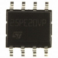
M25PE20-VMN6TP NUMONYX, M25PE20-VMN6TP Datasheet - Page 6

M25PE20-VMN6TP
Manufacturer Part Number
M25PE20-VMN6TP
Description
IC FLASH 2MBIT 75MHZ 8SOIC
Manufacturer
NUMONYX
Series
Forté™r
Datasheet
1.M25PE10-VMN6TP.pdf
(64 pages)
Specifications of M25PE20-VMN6TP
Format - Memory
FLASH
Memory Type
FLASH
Memory Size
2M (256K x 8)
Speed
75MHz
Interface
SPI, 3-Wire Serial
Voltage - Supply
2.7 V ~ 3.6 V
Operating Temperature
-40°C ~ 85°C
Package / Case
8-SOIC (3.9mm Width)
Cell Type
NOR
Density
2Mb
Access Time (max)
8ns
Interface Type
Serial (SPI)
Boot Type
Not Required
Address Bus
1b
Operating Supply Voltage (typ)
3.3V
Operating Temp Range
-40C to 85C
Package Type
SOIC N
Sync/async
Synchronous
Operating Temperature Classification
Industrial
Operating Supply Voltage (min)
2.7V
Operating Supply Voltage (max)
3.6V
Word Size
8b
Number Of Words
256K
Supply Current
8mA
Mounting
Surface Mount
Pin Count
8
Lead Free Status / RoHS Status
Lead free / RoHS Compliant
Other names
M25PE20-VMN6TPTR
Available stocks
Company
Part Number
Manufacturer
Quantity
Price
Company:
Part Number:
M25PE20-VMN6TP
Manufacturer:
MICRON
Quantity:
3 000
Company:
Part Number:
M25PE20-VMN6TP
Manufacturer:
Numonyx
Quantity:
16 500
Part Number:
M25PE20-VMN6TP
Manufacturer:
MICRON/美光
Quantity:
20 000
Description
1
6/64
Description
The M25PE20 and M25PE10 are 2 Mbit (256 Kb × 8 bit) and 1 Mbit (128 Kb × 8 bit) serial
paged Flash memories, respectively. They are accessed by a high speed SPI-compatible
bus.
The memories can be written or programmed 1 to 256 bytes at a time, using the Page Write
or Page Program instruction. The Page Write instruction consists of an integrated Page
Erase cycle followed by a Page Program cycle.
The M25PE20 memory is organized as 4 sectors, each containing 256 pages. Each page is
256 bytes wide. Thus, the whole memory can be viewed as consisting of 1024 pages, or
262,144 bytes.
The M25PE10 memory is organized as 2 sectors, each containing 256 pages. Each page is
256 bytes wide. Thus, the whole memory can be viewed as consisting of 512 pages, or
131, 072 bytes.
The memories can be erased a page at a time, using the Page Erase instruction, a
subsector at a time, using the SubSector Erase instruction, a sector at a time, using the
Sector Erase instruction or as a whole, using the Bulk Erase instruction.
The memory can be write protected by either hardware or software using a mix of volatile
and non-volatile protection features, depending on the application needs. The protection
granularity is of 64 Kbytes (sector granularity).
Important note
This datasheet details the functionality of the M25PE20 and M25PE10 devices, based on
the previous T7X process or based on the current T9HX process (available since July 2007).
Delivery of parts operating with a maximum clock rate of 75 MHz starts from week 8 of
2008.
What are the changes?
The M25PE10/M25PE20 in T9HX process offers the following additional features:
●
●
●
●
●
the whole memory array is partitioned into 4-Kbyte subsectors
five new instructions: Write Status Register (WRSR), Write to Lock Register (WRLR),
Read Lock Register (RDLR), 4-Kbyte SubSector Erase (SSE) and Bulk Erase (BE)
Status Register: 3 bits can be written (BP0, BP1, SRWD)
WP input (pin 3): write protection limits are extended, depending on the value of the
BP0, BP1, SRWD bits. The WP write protection remains the same if bits (BP1, BP0)
are set to (0, 1) or (1, 0)
VFQFPN8 6 × 5 mm package added.
M25PE20, M25PE10


