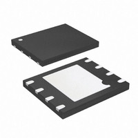
AT25DF641-MWH-Y Atmel, AT25DF641-MWH-Y Datasheet - Page 38

AT25DF641-MWH-Y
Manufacturer Part Number
AT25DF641-MWH-Y
Description
IC FLASH 64MBIT 100MHZ 8VDFN
Manufacturer
Atmel
Datasheet
1.AT25DF641-MWH-T.pdf
(56 pages)
Specifications of AT25DF641-MWH-Y
Format - Memory
FLASH
Memory Type
DataFLASH
Memory Size
64M (32K pages x 256 bytes)
Speed
100MHz
Interface
SPI, 3-Wire Serial
Voltage - Supply
2.7 V ~ 3.6 V
Operating Temperature
-40°C ~ 85°C
Package / Case
8-VDFN
Architecture
Sectored
Interface Type
SPI Serial
Supply Voltage (max)
3.6 V
Supply Voltage (min)
2.7 V
Maximum Operating Current
19 mA
Mounting Style
SMD/SMT
Organization
64 KB x 128
Cell Type
NOR
Density
64Mb
Access Time (max)
5ns
Boot Type
Not Required
Address Bus
1b
Operating Supply Voltage (typ)
3.3V
Operating Temp Range
-40C to 85C
Package Type
VDFN
Sync/async
Synchronous
Operating Temperature Classification
Industrial
Operating Supply Voltage (min)
2.7V
Operating Supply Voltage (max)
3.6V
Supply Current
19mA
Mounting
Surface Mount
Pin Count
8
Lead Free Status / RoHS Status
Lead free / RoHS Compliant
10.2.
38
Write Status Register Byte 1
The Write Status Register Byte 1 command is used to modify the SPRL bit of the Status Register and/or to
perform a Global Protect or Global Unprotect operation. Before the Write Status Register Byte 1 command can be
issued, the Write Enable command must have been previously issued to set the WEL bit in the Status Register to
a logical “1”.
To issue the Write Status Register Byte 1 command, the
must be clocked into the device followed by one byte of data. The one byte of data consists of the SPRL bit value,
a don’t care bit, four data bits to denote whether a Global Protect or Unprotect should be performed, and two
additional don’t care bits (see Table 10-1). Any additional data bytes that are sent to the device will be ignored.
When the
Register will be reset back to a logical “0”. The values of bits five, four, three, and two and the state of the SPRL
bit before the Write Status Register Byte 1 command was executed (the prior state of the SPRL bit) will determine
whether or not a Global Protect or Global Unprotect will be performed. Please refer to “Global Protect/Unprotect”
on page 24 for more details.
The complete one byte of data must be clocked into the device before the
must be deasserted on even byte boundaries (multiples of eight bits); otherwise, the device will abort the
operation, the state of the SPRL bit will not change, no potential Global Protect or Unprotect will be performed,
and the WEL bit in the Status Register will be reset back to the logical “0” state.
If the
SPRL bit to a logical “0” while the
ignored, and the WEL bit in the Status Register will be reset back to the logical “0” state. In order to reset the
SPRL bit to a logical “0”, the
Table 10-3.
Figure 10-2. Write Status Register Byte 1
Atmel AT25DF641
SCK
SO
SPRL
CS
Bit 7
SI
WP
pin is asserted, then the SPRL bit can only be set to a logical “1”. If an attempt is made to reset the
CS
pin is deasserted, the SPRL bit in the Status Register will be modified, and the WEL bit in the Status
Write Status Register Byte 1 Format
Bit 6
X
MS B
HIG H-IMP E DANC E
0
0
0
1
0
2
OPCODE
Bit 5
0
WP
3
0
4
pin must be deasserted.
0
5
Global Protect/Unprotect
WP
0
6
1
Bit 4
7
pin is asserted, then the Write Status Register Byte 1 command will be
MS B
D
8
S TATUS R E GIS TE R IN
X
9
D
10 11
BYTE 1
D
Bit 3
D
12
D
13
X
14 15
X
CS
Bit 2
pin must first be asserted and the opcode of 01h
Bit 1
X
CS
pin is deasserted, and the
Bit 0
X
3680F–DFLASH–4/10
CS
pin


