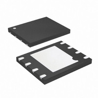
AT25DF641-MWH-Y Atmel, AT25DF641-MWH-Y Datasheet - Page 15

AT25DF641-MWH-Y
Manufacturer Part Number
AT25DF641-MWH-Y
Description
IC FLASH 64MBIT 100MHZ 8VDFN
Manufacturer
Atmel
Datasheet
1.AT25DF641-MWH-T.pdf
(56 pages)
Specifications of AT25DF641-MWH-Y
Format - Memory
FLASH
Memory Type
DataFLASH
Memory Size
64M (32K pages x 256 bytes)
Speed
100MHz
Interface
SPI, 3-Wire Serial
Voltage - Supply
2.7 V ~ 3.6 V
Operating Temperature
-40°C ~ 85°C
Package / Case
8-VDFN
Architecture
Sectored
Interface Type
SPI Serial
Supply Voltage (max)
3.6 V
Supply Voltage (min)
2.7 V
Maximum Operating Current
19 mA
Mounting Style
SMD/SMT
Organization
64 KB x 128
Cell Type
NOR
Density
64Mb
Access Time (max)
5ns
Boot Type
Not Required
Address Bus
1b
Operating Supply Voltage (typ)
3.3V
Operating Temp Range
-40C to 85C
Package Type
VDFN
Sync/async
Synchronous
Operating Temperature Classification
Industrial
Operating Supply Voltage (min)
2.7V
Operating Supply Voltage (max)
3.6V
Supply Current
19mA
Mounting
Surface Mount
Pin Count
8
Lead Free Status / RoHS Status
Lead free / RoHS Compliant
7.3.
3680F–DFLASH–4/10
Figure 7-4.
Block Erase
A block of 4-, 32-, or 64-Kbytes can be erased (all bits set to the logical “1” state) in a single operation by using
one of three different opcodes for the Block Erase command. An opcode of 20h is used for a 4-Kbyte erase, an
opcode of 52h is used for a 32-Kbyte erase, and an opcode of D8h is used for a 64-Kbyte erase. Before a Block
Erase command can be started, the Write Enable command must have been previously issued to the device to
set the WEL bit of the Status Register to a logical “1” state.
To perform a Block Erase, the
be clocked into the device. After the opcode has been clocked in, the three address bytes specifying an address
within the 4-, 32-, or 64-Kbyte block to be erased must be clocked in. Any additional data clocked into the device
will be ignored. When the
block is internally self-timed and should take place in a time of t
Since the Block Erase command erases a region of bytes, the lower order address bits do not need to be
decoded by the device. Therefore, for a 4-Kbyte erase, address bits A11-A0 will be ignored by the device and
their values can be either a logical “1” or “0”. For a 32-Kbyte erase, address bits A14-A0 will be ignored, and for a
64-Kbyte erase, address bits A15-A0 will be ignored by the device. Despite the lower order address bits not being
decoded by the device, the complete three address bytes must still be clocked into the device before the
deasserted, and the
device will abort the operation and no erase operation will be performed.
If the address specified by A23-A0 points to a memory location within a sector that is in the protected or locked
down state, then the Block Erase command will not be executed, and the device will return to the idle state once
the
The WEL bit in the Status Register will be reset back to the logical “0” state if the erase cycle aborts due to an
incomplete address being sent, the
location within the region to be erased is protected or locked down.
While the device is executing a successful erase cycle, the Status Register can be read and will indicate that the
device is busy. For faster throughput, it is recommended that the Status Register be polled rather than waiting the
t
WEL bit in the Status Register will be reset back to the logical “0” state.
The device also incorporates an intelligent erase algorithm that can detect when a byte location fails to erase
properly. If an erase error occurs, it will be indicated by the EPE bit in the Status Register.
BLKE
SCK
SOI
CS
CS
SI
time to determine if the device has finished erasing. At some point before the erase cycle completes, the
pin has been deasserted.
Dual-Input Page Program
HIG H-IMP E DANC E
MS B
1
CS
0
0
1
pin must be deasserted on an even byte boundary (multiples of eight bits); otherwise, the
1
2
OP C ODE
CS
0
3
0
pin is deasserted, the device will erase the appropriate block. The erasing of the
CS
4
0
5
pin must first be asserted and the appropriate opcode (20h, 52h, or D8h) must
1
6
CS
0
7
pin being deasserted on uneven byte boundaries, or because a memory
MS B
A
8
A
9
ADDR E S S B IT S A23-A0
A
10 11
A
A
12
A
A
29 30
A
BLKE
A
31 32
.
MS B
D 6
D 7
DAT A B Y T E 1
INP UT
D 4
D 5
33
D 2
D 3
34
D 0
D 1
35
MS B
D 6
D 7
DAT A B Y T E 2
36
Atmel AT25DF641
INP UT
D 4
D 5
37 38
D 2
D 3
D 0
D 1
39
MS B
D 6
D 7
DAT A B Y T E n
INP UT
D 4
D 5
D 2
D 3
D 0
D 1
CS
pin is
15


