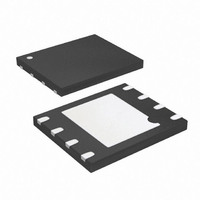
AT25DF641-MWH-Y Atmel, AT25DF641-MWH-Y Datasheet - Page 13

AT25DF641-MWH-Y
Manufacturer Part Number
AT25DF641-MWH-Y
Description
IC FLASH 64MBIT 100MHZ 8VDFN
Manufacturer
Atmel
Datasheet
1.AT25DF641-MWH-T.pdf
(56 pages)
Specifications of AT25DF641-MWH-Y
Format - Memory
FLASH
Memory Type
DataFLASH
Memory Size
64M (32K pages x 256 bytes)
Speed
100MHz
Interface
SPI, 3-Wire Serial
Voltage - Supply
2.7 V ~ 3.6 V
Operating Temperature
-40°C ~ 85°C
Package / Case
8-VDFN
Architecture
Sectored
Interface Type
SPI Serial
Supply Voltage (max)
3.6 V
Supply Voltage (min)
2.7 V
Maximum Operating Current
19 mA
Mounting Style
SMD/SMT
Organization
64 KB x 128
Cell Type
NOR
Density
64Mb
Access Time (max)
5ns
Boot Type
Not Required
Address Bus
1b
Operating Supply Voltage (typ)
3.3V
Operating Temp Range
-40C to 85C
Package Type
VDFN
Sync/async
Synchronous
Operating Temperature Classification
Industrial
Operating Supply Voltage (min)
2.7V
Operating Supply Voltage (max)
3.6V
Supply Current
19mA
Mounting
Surface Mount
Pin Count
8
Lead Free Status / RoHS Status
Lead free / RoHS Compliant
7.2.
3680F–DFLASH–4/10
Figure 7-1.
Figure 7-2.
Dual-Input Byte/Page Program
The Dual-Input Byte/Page Program command is similar to the standard Byte/Page Program command and can be
used to program anywhere from a single byte of data up to 256-bytes of data into previously erased memory
locations. Unlike the standard Byte/Page Program command, however, the Dual-Input Byte/Page Program
command allows two bits of data to be clocked into the device on every clock cycle rather than just one.
Before the Dual-Input Byte/Page Program command can be started, the Write Enable command must have been
previously issued to the device (see “Write Enable” on page 21) to set the Write Enable Latch (WEL) bit of the
Status Register to a logical “1” state. To perform a Dual-Input Byte/Page Program command, an opcode of A2h
must be clocked into the device followed by the three address bytes denoting the first byte location of the memory
array to begin programming at. After the address bytes have been clocked in, data can then be clocked into the
device two bits at a time on both the SOI and SI pins.
The data is always input with the MSB of a byte first, and the MSB is always input on the SOI pin. During the first
clock cycle, bit seven of the first data byte would be input on the SOI pin while bit six of the same data byte would
be input on the SI pin. During the next clock cycle, bits five and four of the first data byte would be input on the
SOI and SI pins, respectively. The sequence would continue with each byte of data being input after every four
clock cycles. Like the standard Byte/Page Program command, all data clocked into the device is stored in an
internal buffer.
SCK
SCK
SO
SO
CS
CS
SI
SI
Byte Program
Page Program
HIG H-IMP E DANC E
MS B
MS B
HIG H-IMP E DANC E
0
0
0
0
0
0
1
1
0
0
2
OP C ODE
2
O P C O DE
0
3
0
3
0
4
0
4
0
5
0
5
1
6
1
6
0
7
0
7
MS B
A
ADDR E S S B IT S A23-A0
MS B
8
A
8
A
9
A
9
A
ADDR E S S B IT S A23-A0
A
10 11
A
A
A
29 30
12
A
A
A
31 32
MS B
D
A
29 30
D
33
DAT A IN B Y T E 1
A
D
34
A
31 32
D
35
MS B
D
D
36
D
D
33
37 38
D
D
34
DAT A IN
D
D
35
39
Atmel AT25DF641
D
36
D
37 38
MS B
D
D
D
D
3 9
DAT A IN B Y T E n
D
D
D
D
D
D
13


