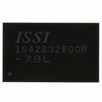
IS42S32800B-7BL ISSI, Integrated Silicon Solution Inc, IS42S32800B-7BL Datasheet - Page 12

IS42S32800B-7BL
Manufacturer Part Number
IS42S32800B-7BL
Description
IC SDRAM 256MBIT 143MHZ 90BGA
Manufacturer
ISSI, Integrated Silicon Solution Inc
Type
SDRAMr
Datasheet
1.IS42S32800B-7BL.pdf
(62 pages)
Specifications of IS42S32800B-7BL
Package / Case
90-BGA
Memory Size
256M (8Mx32)
Format - Memory
RAM
Memory Type
SDRAM
Speed
143MHz
Interface
Parallel
Voltage - Supply
3 V ~ 3.6 V
Operating Temperature
0°C ~ 70°C
Data Bus Width
32 bit
Organization
2 Mbit x 32
Maximum Clock Frequency
143 MHz
Access Time
7 ns
Supply Voltage (max)
3.6 V
Supply Voltage (min)
3 V
Maximum Operating Current
150 mA
Maximum Operating Temperature
+ 70 C
Minimum Operating Temperature
0 C
Mounting Style
SMD/SMT
Density
256Mb
Address Bus
14b
Access Time (max)
5.5ns
Maximum Clock Rate
143MHz
Operating Supply Voltage (typ)
3.3V
Package Type
BGA
Operating Temp Range
0C to 70C
Operating Supply Voltage (max)
3.6V
Operating Supply Voltage (min)
3V
Supply Current
150mA
Pin Count
90
Mounting
Surface Mount
Operating Temperature Classification
Commercial
Lead Free Status / RoHS Status
Lead free / RoHS Compliant
Lead Free Status / RoHS Status
Lead free / RoHS Compliant, Lead free / RoHS Compliant
Other names
706-1024
Available stocks
Company
Part Number
Manufacturer
Quantity
Price
Company:
Part Number:
IS42S32800B-7BL
Manufacturer:
ISSI
Quantity:
1 000
Company:
Part Number:
IS42S32800B-7BL
Manufacturer:
ISSI, Integrated Silicon Solution Inc
Quantity:
10 000
Part Number:
IS42S32800B-7BL
Manufacturer:
ISSI
Quantity:
20 000
Company:
Part Number:
IS42S32800B-7BL-TR
Manufacturer:
ISSI, Integrated Silicon Solution Inc
Quantity:
10 000
Company:
Part Number:
IS42S32800B-7BLI
Manufacturer:
ISSI
Quantity:
1 000
Company:
Part Number:
IS42S32800B-7BLI
Manufacturer:
ISSI, Integrated Silicon Solution Inc
Quantity:
10 000
Company:
Part Number:
IS42S32800B-7BLI-TR
Manufacturer:
ISSI, Integrated Silicon Solution Inc
Quantity:
10 000
IS42S32800B
12
CLK
COMMAND
DQ’s
CLK
COMMAND
CAS# latency=2
t CK2 , DQ’s
Note:The DQMs can remain low in this example if the length of the write burst is 1 or 2.
CAS# latency=3
t CK3 , DQ’s
CLK
DQM
COMMAND
ADDRESS
DQ
The Read command that interrupts a write burst without auto precharge function should be issued one cycle after
the clock edge in which the last data-in element is registered.In order to avoid data contention,input data must
be removed from the DQs at least one clock cycle before the first read data appears on the outputs (refer to the
following figure).Once the Read command is registered,the data inputs will be ignored and writes will not be
executed.
The BankPrecharge/PrechargeAll command that interrupts a write burst without the auto precharge function
should be issued m cycles after the clock edge in which the last data-in element is registered,where m equals tWR/
tCK rounded up to the next whole number.In addition,the DQM signals must be used to mask input data,starting
with the clock edge following the last data-in element and ending with the clock edge on which the BankPrecharge/
PrechargeAll command is entered (refer to the following figure).
: don t care
Write Interrupted by a Write (Burst Length =4,CAS#Latency =2,3)
Write Interrupted by a Read (Burst Length =4,CAS#Latency =2,3)
T0
T0
NOP
NOP
BANK
COL n
WRITE
DIN
T0
n
Input data for the write is masked.
WRITEA
WRITEA
DIN A 0
T 1
T1
DIN A 0
DIN A 0
1 Clk Interval
NOP
n + 1
T1
t WR
WRITEB
READ B
DIN B 0
don’t care
don’t care
T2
T2
Precharge
BANK (S)
T2
DIN B 1
Write to Precharge
T3
don’t care
T3
NOP
NOP
NOP
DI N
T3
DIN B 2
T4
NOP
T4
NOP
t RP
DOUT B 0
NOP
Input data must be removed from the DQs at least one clock
cycle before the Read data appears on the outputs to avoid
data contention.
T4
DIN B 3
T5
T5
NOP
NOP
DOUT B 0
DOUT B 1
Activate
ROW
T5
T6
NOP
T6
NOP
DOUT B 2
DOUT B 1
Integrated Silicon Solution, Inc.
NOP
T6
T7
NOP
T7
DOUT B 3
NOP
DOUT B 2
T8
NOP
T8
NOP
DOUT B 3
07/21/09
Rev. F


