FXL2TD245L10X Fairchild Semiconductor, FXL2TD245L10X Datasheet - Page 7
FXL2TD245L10X
Manufacturer Part Number
FXL2TD245L10X
Description
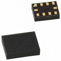
TRANSLATOR 2BIT LV DL 10MICROPAK
Manufacturer
Fairchild Semiconductor
Datasheet
1.FXL2TD245L10X.pdf
(12 pages)
Specifications of FXL2TD245L10X
Logic Function
Translator, 3-State
Number Of Bits
2
Input Type
Voltage
Output Type
Voltage
Number Of Channels
1
Number Of Outputs/channel
2
Differential - Input:output
No/No
Propagation Delay (max)
3.5ns
Voltage - Supply
1.1 V ~ 3.6 V
Operating Temperature
-40°C ~ 85°C
Package / Case
10-MicroPak™
Supply Voltage
1.1 V ~ 3.6 V
Logic Type
CMOS
Logic Family
FXL
Number Of Channels Per Chip
2
High Level Output Current
- 24 mA
Low Level Output Current
24 mA
Propagation Delay Time
24 ns
Supply Voltage (max)
3.6 V
Supply Voltage (min)
1.1 V
Maximum Operating Temperature
+ 85 C
Function
Bus Transceiver
Input Bias Current (max)
20 uA
Minimum Operating Temperature
- 40 C
Mounting Style
SMD/SMT
Number Of Circuits
1
Polarity
Non-Inverting
Operating Supply Voltage (typ)
1.8/2.5/3.3V
Number Of Elements
1
Package Type
MicroPak W
Logical Function
Bus Transceiver
Operating Supply Voltage (min)
1.1V
Operating Supply Voltage (max)
3.6V
Technology
CMOS
Operating Temp Range
-40C to 85C
Operating Temperature Classification
Industrial
Mounting
Surface Mount
Pin Count
10
Lead Free Status / RoHS Status
Lead free / RoHS Compliant
Data Rate
-
Lead Free Status / Rohs Status
Lead free / RoHS Compliant
Other names
FXL2TD245L10XTR
Available stocks
Company
Part Number
Manufacturer
Quantity
Price

Part Number:
FXL2TD245L10X
Manufacturer:
FAIRCHILD/仙童
Quantity:
20 000


©2005 Fairchild Semiconductor Corporation
FXL2TD245 Rev. 1.0.4
AC Electrical Characteristics
V
V
Capacitance
Symbol
t
t
t
t
t
t
Symbol
Symbol
CCA
CCA
PLH
PZH
PHZ
PLH
PZH
PHZ
C
C
C
I/O
PD
, t
, t
IN
, t
, t
, t
, t
= 1.4V to 1.6V
PHL
= 1.1V to 1.3V
PHL
PZL
PLZ
PZL
PLZ
Input Capacitance Control Pins (OE, T/Rn)
Input/Output Capacitance A
Power Dissipation Capacitance
Propagation Delay A to B
Propagation Delay B to A
Output Enable OE to B
Output Enable OE to A
Output Disable OE to B
Output Disable OE to A
Propagation Delay A to B
Propagation Delay B to A
Output Disable OE to B
Output Disable OE to A
Output Enable OE to B
Output Enable OE to A
Parameter
Parameter
Parameter
n
, B
3.0V to 3.6V
Min.
3.0V to 3.6V
Min.
0.5
0.6
1.1
1.0
0.4
1.0
0.8
1.4
1.0
2.0
1.0
2.0
n
V
V
Ports
CCB
CCB
(Continued)
Max.
Max.
13.0
22.0
12.0
22.0
15.0
15.0
4.3
6.8
7.5
7.5
6.1
6.0
=
=
2.3V to 2.7V
V
V
V
F = 10MHz
2.3V to 2.7V
Min.
Min.
0.5
0.8
1.1
1.0
0.4
1.0
CCA
CCA
CCA
1.0
1.4
1.0
2.0
0.7
2.0
V
V
CCB
CCB
= V
= V
= V
7
Max.
Max.
22.0
22.0
12.0
CCB
CCB
CCB
4.8
6.9
7.6
7.5
6.2
6.0
=
7.0
9.0
7.0
=
T
T
A
= 3.3V, V
= 3.3V, V
= 3.3V, V
A
Conditions
= -40°C to +85°C
= -40°C to +85°C
Min.
Min.
1.0
0.9
1.3
1.0
0.9
1.0
1.2
1.5
2.0
2.0
1.0
2.0
1.65V to
1.65V to
V
V
1.95V
1.95V
CCB
CCB
I
I
I
= 0V or V
= 0V or V
= 0V or V
Max.
Max.
22.0
10.0
22.0
12.0
6.0
7.1
7.7
7.5
6.2
6.0
=
8.0
8.0
=
CCA/B
CCA/B
CC
1.4V to 1.6V
1.4V to 1.6V
Min.
Min.
1.0
1.0
1.4
1.0
1.5
1.0
1.3
1.5
2.0
2.0
2.0
2.0
,
V
V
CCB
CCB
Max.
Max.
22.0
11.0
22.0
10.0
12.0
7.3
7.3
7.9
7.5
7.5
6.0
=
=
9.5
T
A
Typical
1.1V to 1.3V
1.1V to 1.3V
Min.
Min.
1.5
1.3
2.0
1.0
2.0
1.0
= +25°C
2.0
2.0
2.0
2.0
2.0
2.0
20.0
4.0
5.0
V
V
CCB
CCB
Max.
Max.
22.0
20.0
18.0
24.0
24.0
24.0
22.0
20.0
12.0
www.fairchildsemi.com
9.5
=
7.5
6.0
=
Units
Units
Units
pF
pF
pF
ns
ns
ns
ns
ns
ns
Related parts for FXL2TD245L10X
Image
Part Number
Description
Manufacturer
Datasheet
Request
R

Part Number:
Description:
Fairchild Semiconductor [IGBT MODULE]
Manufacturer:
Fairchild Semiconductor
Datasheet:

Part Number:
Description:
Discrete Semiconductor Modules
Manufacturer:
Fairchild Semiconductor
Part Number:
Description:
Discrete Semiconductor Modules
Manufacturer:
Fairchild Semiconductor
Part Number:
Description:
This N-Channel MOSFET is produced using Fairchild Semiconductor’s advanced Power Trench® process
Manufacturer:
Fairchild Semiconductor
Datasheet:
Part Number:
Description:
This N-Channel MOSFET is produced using Fairchild Semiconductor’s advanced Power Trench® process
Manufacturer:
Fairchild Semiconductor
Datasheet:
Part Number:
Description:
This N-Channel MOSFET is produced using Fairchild Semiconductor’s advanced PowerTrench® process
Manufacturer:
Fairchild Semiconductor
Datasheet:
Part Number:
Description:
This N-Channel MOSFET is produced using Fairchild Semiconductor’s advanced PowerTrench® process
Manufacturer:
Fairchild Semiconductor
Datasheet:
Part Number:
Description:
This N-Channel MOSFET is produced using Fairchild Semiconductor’s advanced Power Trench® process
Manufacturer:
Fairchild Semiconductor
Datasheet:
Part Number:
Description:
This N-Channel logic Level MOSFETs are produced using Fairchild Semiconductor‘s advanced Power Trench® process that has been special tailored to minimize the on-state resistance and yet maintain superior switching performance
Manufacturer:
Fairchild Semiconductor
Datasheet:
Part Number:
Description:
This N-Channel MOSFET is produced using Fairchild Semiconductor’s advanced Power Trench® process
Manufacturer:
Fairchild Semiconductor
Datasheet:
Part Number:
Description:
This N-Channel SyncFET™ is produced using Fairchild Semiconductor’s advanced PowerTrench® process
Manufacturer:
Fairchild Semiconductor
Datasheet:
Part Number:
Description:
This N-Channel SyncFET™ is produced using Fairchild Semiconductor’s advanced PowerTrench® process
Manufacturer:
Fairchild Semiconductor
Datasheet:
Part Number:
Description:
This N-Channel SyncFET™ is produced using Fairchild Semiconductor’s advanced PowerTrench® process
Manufacturer:
Fairchild Semiconductor
Datasheet:
Part Number:
Description:
This N-Channel logic Level MOSFETs are produced using Fairchild Semiconductor‘s advanced Power Trench® process that has been special tailored to minimize the on-state resistance and yet maintain superior switching performance
Manufacturer:
Fairchild Semiconductor
Datasheet:
Part Number:
Description:
This N-Channel MOSFET is produced using Fairchild Semiconductor’s advanced Power Trench® process that has been especially tailored to minimize the on-state resistance and yet maintain superior switching performance
Manufacturer:
Fairchild Semiconductor
Datasheet: