74VHC161284MTDX Fairchild Semiconductor, 74VHC161284MTDX Datasheet
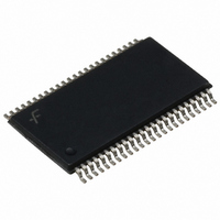
TXRX BIDIRECT IEEE 48TSSOP

74VHC161284MTDX

Manufacturer Part Number
74VHC161284MTDX
Description
TXRX BIDIRECT IEEE 48TSSOP
Manufacturer
Fairchild Semiconductor
Series
74VHCr
Datasheet

Specifications of 74VHC161284MTDX

Logic Type
IEEE STD 1284 Translation Transceiver
Supply Voltage
4.5 V ~ 5.5 V
Number Of Bits
8
Operating Temperature
-40°C ~ 85°C
Mounting Type
Surface Mount
Package / Case
48-SSOP
Logic Family
74VHC
Maximum Operating Temperature
85 C
Function
IEEE 16284 Trans
Minimum Operating Temperature
- 40 C
Mounting Style
SMD/SMT
Lead Free Status / RoHS Status
Lead free / RoHS Compliant

Available stocks

Company
Part Number
Manufacturer
Quantity
Price
Part Number:
74VHC161284MTDX
Manufacturer:
FSC
Quantity:
1 181
Part Number:
74VHC161284MTDX
Manufacturer:
HAR
Quantity:
14
Part Number:
74VHC161284MTDX
Manufacturer:
FAIRCHILD/仙童
Quantity:
20 000
© 2005 Fairchild Semiconductor Corporation
74VHC161284MEA
74VHC161284MTD
Ordering Number Package Number
74VHC161284
IEEE 1284 Transceiver
General Description
The VHC161284 contains eight bidirectional data buffers
and eleven control/status buffers to implement a full
IEEE 1284 compliant interface. The device supports the
IEEE 1284 standard and is intended to be used in
Extended Capabilities Port mode (ECP). The pinout allows
for easy connection from the Peripheral (A-side) to the
Host (cable side).
Outputs on the cable side can be configured to be either
open drain or high drive (
down series termination resistance of these outputs on the
cable side is optimized to drive an external cable. In addi-
tion, all inputs (except HLH) and outputs on the cable side
contain internal pull-up resistors connected to the V
ply to provide proper termination and pull-ups for open
drain mode.
Outputs on the Peripheral side are standard LOW-drive
CMOS outputs. The DIR input controls data flow on the A
A
Ordering Code:
Surface mount packages are also available on Tape and Reel. Specify by appending the suffix letter “X” to the ordering code.
Logic Symbol
8
/B
1
–B
8
transceiver pins.
MS48A
MTD48
r
14 mA). The pull-up and pull-
48-Lead Small Shrink Outline Package (SSOP), JEDEC MO-118, 0.300" Wide
48-Lead Thin Shrink Small Outline Package (TSSOP), JEDEC MO-153, 6.1mm Wide
DS500098
CC
sup-
1
Features
Connection Diagram
Supports IEEE 1284 Level 1 and Level 2 signaling
standards for bidirectional parallel communications
between personal computers and printing peripherals
Replaces the function of two (2) 74ACT1284 devices
All inputs have hysteresis to provide noise margin
B and Y output resistance optimized to drive external
cable
B and Y outputs in high impedance mode during power
down
Inputs and outputs on cable side have internal pull-up
resistors
Flow-through pin configuration allows easy interface
between the Peripheral and Host
Package Description
February 1998
Revised June 2005
www.fairchildsemi.com

Related parts for 74VHC161284MTDX

74VHC161284MTDX Summary of contents

Page 1

... Thin Shrink Small Outline Package (TSSOP), JEDEC MO-153, 6.1mm Wide Surface mount packages are also available on Tape and Reel. Specify by appending the suffix letter “X” to the ordering code. Logic Symbol © 2005 Fairchild Semiconductor Corporation Features Supports IEEE 1284 Level 1 and Level 2 signaling ...

Page 2

Pin Descriptions Pin Names Description HD HIGH Drive Enable Input (Active HIGH) DIR Direction Control Input A –A Inputs or Outputs –B Inputs or Outputs –A Inputs –Y Outputs 9 13 ...

Page 3

Absolute Maximum Ratings Supply Voltage V CC Input Voltage (V ) (Note –A , PLH , DIR – –C , HLH 0. ...

Page 4

DC Electrical Characteristics Symbol Parameter V Maximum LOW Level Output Voltage OL RD Maximum Output Impedance Minimum Output Impedance RP Maximum Pull-Up Resistance Minimum Pull-Up Resistance I Maximum Input Current in HIGH State IH I Maximum Input Current in LOW ...

Page 5

AC Electrical Characteristics Symbol Parameter t A – –B PHL – –B PLH – –A PHL ...

Page 6

AC Loading and Waveforms d Pulse Generator for all pulses: Rate 1.0 MHz; Z FIGURE 1. Part and Propagation Delay Load and Waveforms FIGURE 2. Port and Output ...

Page 7

AC Loading and Waveforms FIGURE 4. Port and Slew Test Load and Waveforms FIGURE 5. Part and Slew Test Load and Waveforms FIGURE 6. t and ...

Page 8

AC Loading and Waveforms FIGURE 7. t PHZ FIGURE 8. t PZH www.fairchildsemi.com (Continued) and t Test Load and Waveforms, DIR to A PLZ and t Test Load and Waveforms, DIR to A PZL 8 – –A 1 ...

Page 9

AC Loading and Waveforms FIGURE 9. t and t PHZ (Continued) Test Load and Waveforms, DIR to B –B PLZ www.fairchildsemi.com ...

Page 10

Physical Dimensions inches (millimeters) unless otherwise noted 48-Lead Small Shrink Outline Package (SSOP), JEDEC MO-118, 0.300" Wide www.fairchildsemi.com Package Number MS48A 10 ...

Page 11

Physical Dimensions inches (millimeters) unless otherwise noted (Continued) 48-Lead Thin Shrink Small Outline Package (TSSOP), JEDEC MO-153, 6.1mm Wide Fairchild does not assume any responsibility for use of any circuitry described, no circuit patent licenses are implied and Fairchild reserves ...

Related keywords