ADG3245BCP-REEL7 Analog Devices Inc, ADG3245BCP-REEL7 Datasheet
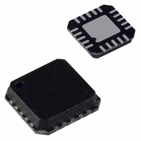
IC SW BUS 2.5/3.3V 8BIT 20LFCSP

ADG3245BCP-REEL7

Manufacturer Part Number
ADG3245BCP-REEL7
Description
IC SW BUS 2.5/3.3V 8BIT 20LFCSP
Manufacturer
Analog Devices Inc
Type
Bus Switchr
Datasheet

Specifications of ADG3245BCP-REEL7

Rohs Status
RoHS non-compliant
Circuit
8 x 1:1
Independent Circuits
1
Voltage Supply Source
Single Supply
Voltage - Supply
2.5V, 3.3V
Operating Temperature
-40°C ~ 85°C
Mounting Type
Surface Mount
Package / Case
20-LFCSP
Number Of Bits
8
Number Of Elements
1
Technology
CMOS
High Level Output Current
-25mA
Propagation Delay Time
4.8ns
Operating Temp Range
-40C to 85C
Operating Temperature Classification
Industrial
Operating Supply Voltage (min)
2.3V
Operating Supply Voltage (typ)
2.5/3.3V
Operating Supply Voltage (max)
3.6V
Quiescent Current
1.2mA
Pin Count
20
Mounting
Surface Mount
Current - Output High, Low
-
Lead Free Status / RoHS Status
Not Compliant
GENERAL DESCRIPTION
The ADG3245 is a 2.5 V or 3.3 V, 8-bit, 2-port digital switch.
It is designed on Analog Devices’ low voltage CMOS process,
which provides low power dissipation yet gives high switching
speed and very low on resistance, allowing inputs to be connected
to outputs without additional propagation delay or generating
additional ground bounce noise.
The switches are enabled by means of the bus enable (BE) input
signal. These digital switches allow bidirectional signals to be
switched when ON. In the OFF condition, signal levels up to
the supplies are blocked.
This device is ideal for applications requiring level translation.
When operated from a 3.3 V supply, level translation from 3.3 V
inputs to 2.5 V outputs is allowed. Similarly, if the device is
operated from a 2.5 V supply and 2.5 V inputs are applied, the
device will translate the outputs to 1.8 V. In addition to this, a
level translating select pin (SEL) is included. When SEL is low,
V
3.3 V inputs and 1.8 V outputs. This makes the device suited to
applications requiring level translation between different supplies,
such as converter to DSP/microcontroller interfacing.
REV. 0
Information furnished by Analog Devices is believed to be accurate and
reliable. However, no responsibility is assumed by Analog Devices for its
use, nor for any infringements of patents or other rights of third parties that
may result from its use. No license is granted by implication or otherwise
under any patent or patent rights of Analog Devices. Trademarks and
registered trademarks are the property of their respective companies.
CC
FEATURES
225 ps Propagation Delay through the Switch
4.5
Data Rate 1.244 Gbps
2.5 V/3.3 V Supply Operation
Selectable Level Shifting/Translation
Level Translation
Small Signal Bandwidth 610 MHz
20-Lead TSSOP and LFCSP Packages
APPLICATIONS
3.3 V to 1.8 V Voltage Translation
3.3 V to 2.5 V Voltage Translation
2.5 V to 1.8 V Voltage Translation
Bus Switching
Bus Isolation
Hot Swap
Hot Plug
Analog Switch Applications
is reduced internally, allowing for level translation between
3.3 V to 2.5 V
3.3 V to 1.8 V
2.5 V to 1.8 V
Switch Connection between Ports
PRODUCT HIGHLIGHTS
1. 3.3 V or 2.5 V supply operation
2. Extremely low propagation delay through switch
3. 4.5 W switches connect inputs to outputs
4. Level/voltage translation
5. 20-lead TSSOP and LFCSP (4 mm ¥ 4 mm) packages
One Technology Way, P.O. Box 9106, Norwood, MA 02062-9106, U.S.A.
Tel: 781/329-4700
Fax: 781/326-8703
Level Translating, Bus Switch
A0
A7
BE
FUNCTIONAL BLOCK DIAGRAM
2.5 V/3.3 V, 8-Bit, 2-Port
© 2003 Analog Devices, Inc. All rights reserved.
ADG3245
www.analog.com
B0
B7

Related parts for ADG3245BCP-REEL7

ADG3245BCP-REEL7 Summary of contents

Page 1

FEATURES 225 ps Propagation Delay through the Switch 4.5 Switch Connection between Ports Data Rate 1.244 Gbps 2.5 V/3.3 V Supply Operation Selectable Level Shifting/Translation Level Translation 3 2 1 ...

Page 2

ADG3245–SPECIFICATIONS Parameter DC ELECTRICAL CHARACTERISTICS Input High Voltage Input Low Voltage Input Leakage Current OFF State Leakage Current ON State Leakage Current Maximum Pass Voltage 3 CAPACITANCE A Port Off Capacitance B Port Off Capacitance A, B Port On Capacitance ...

Page 3

... Industrial (B Version –40°C to +85°C Storage Temperature Range . . . . . . . . . . . . –65°C to +150°C Junction Temperature . . . . . . . . . . . . . . . . . . . . . . . . . . 150°C Model Temperature Range ADG3245BCP –40°C to +85°C ADG3245BCP-REEL7 –40°C to +85°C ADG3245BRU –40°C to +85°C ADG3245BRU-REEL7 –40°C to +85°C Table I. Pin Description ...

Page 4

ADG3245 V Positive Power Supply Voltage. CC GND Ground (0 V) Reference. V Minimum Input Voltage for Logic 1. INH V Maximum Input Voltage for Logic 0. INL I Input Leakage Current at the Control Inputs OFF State ...

Page 5

SEL = 3. 3. 0.5 1.0 1.5 2.0 2.5 3.0 3 ...

Page 6

ADG3245 3 2 2.0 = 3.3V; SEL = 1.5 = SEL = 3. 1.0 0.5 = SEL = 2. ...

Page 7

SEL = 3. p 20dB ATTENUATION EYE WIDTH = ((CLOCK PERIOD – 55 JITTER p-p)/CLOCK PERIOD) 100% 50 0.5 0.6 0.7 0.8 0.9 ...

Page 8

ADG3245 For the following load circuit and waveforms, the notation that is used OUT PULSE D.U.T. GENERATOR R T NOTES t PULSE GENERATOR FOR ALL PULSES: 2.5ns, R FREQUENCY 10MHz. C INCLUDES BOARD, ...

Page 9

BUS SWITCH APPLICATIONS Mixed Voltage Operation, Level Translation Bus switches can be used to provide an ideal solution for inter- facing between mixed voltage systems. The ADG3245 is suitable for applications where voltage translation from 3.3 V technology to a ...

Page 10

ADG3245 V OUT 3.3V SUPPLY SEL = 0V 1.8V 0V SWITCH 3.3V INPUT Figure 10. 3 1.8 V Voltage Translation, SEL = 0 V Bus Isolation A common requirement of bus architectures is low capacitance loading of the ...

Page 11

PIN 1 INDICATOR 1.00 0.90 0.80 SEATING PLANE 20-Lead Thin Shrink Small Outline Package [TSSOP] 0.15 0.05 COPLANARITY 0.10 REV. 0 OUTLINE DIMENSIONS 20-Lead Lead Frame Chip Scale Package [LFCSP Body (CP-20) Dimensions shown in millimeters ...

Page 12

–12– ...

Related keywords