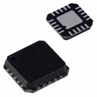
ADG3245BCP-REEL7 Analog Devices Inc, ADG3245BCP-REEL7 Datasheet - Page 4

ADG3245BCP-REEL7
Manufacturer Part Number
ADG3245BCP-REEL7
Description
IC SW BUS 2.5/3.3V 8BIT 20LFCSP
Manufacturer
Analog Devices Inc
Type
Bus Switchr
Datasheet
1.ADG3245BRUZ-REEL7.pdf
(12 pages)
Specifications of ADG3245BCP-REEL7
Rohs Status
RoHS non-compliant
Circuit
8 x 1:1
Independent Circuits
1
Voltage Supply Source
Single Supply
Voltage - Supply
2.5V, 3.3V
Operating Temperature
-40°C ~ 85°C
Mounting Type
Surface Mount
Package / Case
20-LFCSP
Number Of Bits
8
Number Of Elements
1
Technology
CMOS
High Level Output Current
-25mA
Propagation Delay Time
4.8ns
Operating Temp Range
-40C to 85C
Operating Temperature Classification
Industrial
Operating Supply Voltage (min)
2.3V
Operating Supply Voltage (typ)
2.5/3.3V
Operating Supply Voltage (max)
3.6V
Quiescent Current
1.2mA
Pin Count
20
Mounting
Surface Mount
Current - Output High, Low
-
Lead Free Status / RoHS Status
Not Compliant
ADG3245
V
GND
V
V
I
I
I
V
R
C
C
C
I
t
t
t
Max Data Rate
Channel Jitter
f
I
CC
PLH
PZH
PHZ
BE
OZ
OL
CC
INH
INL
P
R
I
ON
X
X
IN
CC
ON
OFF
ON
, t
, t
, t
PHL
PZL
PLZ
Positive Power Supply Voltage.
Ground (0 V) Reference.
Minimum Input Voltage for Logic 1.
Maximum Input Voltage for Logic 0.
Input Leakage Current at the Control Inputs.
OFF State Leakage Current. It is the maximum leakage current at the switch pin in the OFF state.
ON State Leakage Current. It is the maximum leakage current at the switch pin in the ON state.
Maximum Pass Voltage. The maximum pass voltage relates to the clamped output voltage of an NMOS device
when the switch input voltage is equal to the supply voltage.
Ohmic Resistance Offered by a Switch in the ON State. It is measured at a given voltage by forcing a specified
amount of current through the switch.
On Resistance Match between Any Two Channels, i.e., R
OFF Switch Capacitance.
ON Switch Capacitance.
Control Input Capacitance. This consists of BE and SEL.
Quiescent Power Supply Current. This current represents the leakage current between the V
It is measured when all control inputs are at a logic HIGH or LOW level and the switches are OFF.
Extra power supply current component for the BE control input when the input is not driven at the supplies.
Data Propagation Delay through the Switch in the ON State. Propagation delay is related to the RC time constant
R
Bus Enable Times. These are the times taken to cross the V
in response to the control signal, BE.
Bus Disable Times. This is the time taken to place the switch in the high impedance OFF state in response to the control
signal. It is measured as the time taken for the output voltage to change by V from the original quiescent level,
with reference to the logic level transition at the control input. (Refer to Figure 3 for enable and disable times.)
Maximum Rate at which Data Can Be Passed through the Switch.
Peak-to-Peak Value of the Sum of the Deterministic and Random Jitter of the Switch Channel.
Operating Frequency of Bus Enable. This is the maximum frequency at which bus enable (BE) can be toggled.
ON
¥ C
L
, where C
L
is the load capacitance.
TERMINOLOGY
–4–
ON
T
Max – R
voltage at the switch output when the switch turns on
ON
Min.
CC
and ground pins.
REV. 0


