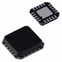
ADG3245BCP-REEL7 Analog Devices Inc, ADG3245BCP-REEL7 Datasheet - Page 9

ADG3245BCP-REEL7
Manufacturer Part Number
ADG3245BCP-REEL7
Description
IC SW BUS 2.5/3.3V 8BIT 20LFCSP
Manufacturer
Analog Devices Inc
Type
Bus Switchr
Datasheet
1.ADG3245BRUZ-REEL7.pdf
(12 pages)
Specifications of ADG3245BCP-REEL7
Rohs Status
RoHS non-compliant
Circuit
8 x 1:1
Independent Circuits
1
Voltage Supply Source
Single Supply
Voltage - Supply
2.5V, 3.3V
Operating Temperature
-40°C ~ 85°C
Mounting Type
Surface Mount
Package / Case
20-LFCSP
Number Of Bits
8
Number Of Elements
1
Technology
CMOS
High Level Output Current
-25mA
Propagation Delay Time
4.8ns
Operating Temp Range
-40C to 85C
Operating Temperature Classification
Industrial
Operating Supply Voltage (min)
2.3V
Operating Supply Voltage (typ)
2.5/3.3V
Operating Supply Voltage (max)
3.6V
Quiescent Current
1.2mA
Pin Count
20
Mounting
Surface Mount
Current - Output High, Low
-
Lead Free Status / RoHS Status
Not Compliant
BUS SWITCH APPLICATIONS
Mixed Voltage Operation, Level Translation
Bus switches can be used to provide an ideal solution for inter-
facing between mixed voltage systems. The ADG3245 is suitable
for applications where voltage translation from 3.3 V technology
to a lower voltage technology is needed. This device can translate
from 3.3 V to 1.8 V, from 2.5 V to 1.8 V, or bidirectionally
from 3.3 V directly to 2.5 V.
Figure 4 shows a block diagram of a typical application in which
a user needs to interface between a 3.3 V ADC and a 2.5 V
microprocessor. The microprocessor may not have 3.3 V toler-
ant inputs, therefore placing the ADG3245 between the two
devices allows the devices to communicate easily. The bus
switch directly connects the two blocks, thus introducing
minimal propagation delay, timing skew, or noise.
3.3 V to 2.5 V Translation
When V
0 V to V
within a voltage threshold below the V
In this case, the output will be limited to 2.5 V, as shown in
Figure 6.
This device can be used for translation from 2.5 V to 3.3 V
devices and also between two 3.3 V devices.
REV. 0
Figure 5. 3.3 V to 2.5 V Voltage Translation, SEL = V
Figure 6. 3.3 V to 2.5 V Voltage Translation, SEL = V
Figure 4. Level Translation between a 3.3 V ADC
and a 2.5 V Microprocessor
CC
CC
3.3V ADC
is 3.3 V (SEL = 3.3 V) and the input signal range is
, the maximum output signal will be clamped to
3.3V
2.5V
3.3V
2.5V
V
0V
OUT
ADG3245
3.3V
SWITCH
INPUT
3.3V
3.3V SUPPLY
SEL = 3.3V
3.3V
CC
MICROPROCESSOR
supply.
V
IN
2.5V
2.5V
2.5V
2.5V
CC
CC
–9–
2.5 V to 1.8 V Translation
When V
0 V to V
to within a voltage threshold below the V
In this case, the output will be limited to approximately
1.8 V, as shown in Figure 7.
3.3 V to 1.8 V Translation
The ADG3245 offers the option of interfacing between a 3.3 V
device and a 1.8 V device. This is possible through use of the
SEL pin.
SEL pin: An active low control pin. SEL activates internal
circuitry in the ADG3245 that allows voltage translation
between 3.3 V devices and 1.8 V devices.
When V
maximum output signal will be clamped to 1.8 V, as shown in
Figure 9. To do this, the SEL pin must be tied to Logic 0. If
SEL is unused, it should be tied directly to V
Figure 7. 2.5 V to 1.8 V Voltage Translation, SEL = 2.5 V
Figure 8. 2.5 V to 1.8 V Voltage Translation, SEL = V
Figure 9. 3.3 V to 1.8 V Voltage Translation, SEL = 0 V
CC
CC
CC
, the maximum output signal will, as before, be clamped
is 2.5 V (SEL = 2.5 V) and the input signal range is
is 3.3 V and the input signal range is 0 V to V
2.5V
3.3V
1.8V
V
0V
OUT
ADG3245
ADG3245
SWITCH
INPUT
3.3V
2.5V
2.5V SUPPLY
SEL = 2.5V
2.5V
CC
V
supply.
IN
ADG3245
CC
.
1.8V
1.8V
CC
, the
CC
CC


