CD4066BCM Fairchild Semiconductor, CD4066BCM Datasheet - Page 4
CD4066BCM
Manufacturer Part Number
CD4066BCM
Description
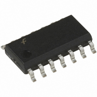
IC SWITCH BILATERAL QUAD 14-SOIC
Manufacturer
Fairchild Semiconductor
Series
4000Br
Type
Bilateral, FET Switchesr
Datasheet
1.CD4066BCM.pdf
(9 pages)
Specifications of CD4066BCM
Circuit
1 x 1:1
Independent Circuits
4
Voltage Supply Source
Dual Supply
Voltage - Supply
3 V ~ 15 V
Operating Temperature
-55°C ~ 125°C
Mounting Type
Surface Mount
Package / Case
14-SOIC (3.9mm Width), 14-SOL
Switch Configuration
SPST
On Resistance (max)
1050 Ohms
On Time (max)
125 ns
Off Time (max)
125 ns
Supply Voltage (max)
15 V
Supply Voltage (min)
3 V
Maximum Power Dissipation
500 mW
Maximum Operating Temperature
+ 125 C
Mounting Style
SMD/SMT
Minimum Operating Temperature
- 55 C
Propagation Delay Time
55 ns
Multiplexer Configuration
Quad SPST
Number Of Inputs
4
Number Of Outputs
4
Number Of Channels
4
Analog Switch On Resistance
1050@5VOhm
Analog Switch Turn On Time
125ns
Analog Switch Turn Off Time
125ns
Package Type
SOIC N
Power Supply Requirement
Single
Single Supply Voltage (min)
3V
Single Supply Voltage (typ)
5/9/12V
Single Supply Voltage (max)
15V
Dual Supply Voltage (min)
Not RequiredV
Dual Supply Voltage (typ)
Not RequiredV
Dual Supply Voltage (max)
Not RequiredV
Power Dissipation
500mW
Mounting
Surface Mount
Pin Count
14
Operating Temp Range
-55C to 125C
Operating Temperature Classification
Military
Dc
08+
Lead Free Status / RoHS Status
Lead free / RoHS Compliant
Current - Output High, Low
-
Lead Free Status / Rohs Status
Lead free / RoHS Compliant
Available stocks
Company
Part Number
Manufacturer
Quantity
Price

Part Number:
CD4066BCM
Manufacturer:
FAIRCHILD/仙童
Quantity:
20 000
Part Number:
CD4066BCMX
Manufacturer:
NS/国半
Quantity:
20 000


www.fairchildsemi.com
Typical Performance Characteristics
Special Considerations
In applications where separate power sources are used to
drive V
should exceed V
CD4066BC bilateral switches). This provision avoids any
permanent current flow or clamp action of the V
when power is applied or removed from CD4066BC.
In certain applications, the external load-resistor current
may include both V
DD
and the signal input, the V
“ON” Resistance as a Function
“ON” Resistance vs Signal
DD
Voltage for T
/R
of Temperature for
DD
V
L
DD
(R
L
and signal-line components. To
V
SS
effective external load of the 4
A
10V
25 C
DD
current capability
DD
supply
4
avoid drawing V
terminals 1, 4, 8 or 11, the voltage drop across the bidirec-
tional switch must not exceed 0.6V at T
T
No V
flows into terminals 2, 3, 9 or 10.
A
25 C (calculated from R
DD
current will flow through R
“ON” Resistance as a Function
“ON” Resistance as a Function
DD
of Temperature for
of Temperature for
current when switch current flows into
V
V
DD
DD
V
V
SS
SS
ON
values shown).
15V
5V
L
if the switch current
A
25 C, or 0.4V at
Related parts for CD4066BCM
Image
Part Number
Description
Manufacturer
Datasheet
Request
R

Part Number:
Description:
Fairchild Semiconductor [IGBT MODULE]
Manufacturer:
Fairchild Semiconductor
Datasheet:

Part Number:
Description:
Discrete Semiconductor Modules
Manufacturer:
Fairchild Semiconductor
Part Number:
Description:
Discrete Semiconductor Modules
Manufacturer:
Fairchild Semiconductor
Part Number:
Description:
This N-Channel MOSFET is produced using Fairchild Semiconductor’s advanced Power Trench® process
Manufacturer:
Fairchild Semiconductor
Datasheet:
Part Number:
Description:
This N-Channel MOSFET is produced using Fairchild Semiconductor’s advanced Power Trench® process
Manufacturer:
Fairchild Semiconductor
Datasheet:
Part Number:
Description:
This N-Channel MOSFET is produced using Fairchild Semiconductor’s advanced PowerTrench® process
Manufacturer:
Fairchild Semiconductor
Datasheet:
Part Number:
Description:
This N-Channel MOSFET is produced using Fairchild Semiconductor’s advanced PowerTrench® process
Manufacturer:
Fairchild Semiconductor
Datasheet:
Part Number:
Description:
This N-Channel MOSFET is produced using Fairchild Semiconductor’s advanced Power Trench® process
Manufacturer:
Fairchild Semiconductor
Datasheet:
Part Number:
Description:
This N-Channel logic Level MOSFETs are produced using Fairchild Semiconductor‘s advanced Power Trench® process that has been special tailored to minimize the on-state resistance and yet maintain superior switching performance
Manufacturer:
Fairchild Semiconductor
Datasheet:
Part Number:
Description:
This N-Channel MOSFET is produced using Fairchild Semiconductor’s advanced Power Trench® process
Manufacturer:
Fairchild Semiconductor
Datasheet:
Part Number:
Description:
This N-Channel SyncFET™ is produced using Fairchild Semiconductor’s advanced PowerTrench® process
Manufacturer:
Fairchild Semiconductor
Datasheet:
Part Number:
Description:
This N-Channel SyncFET™ is produced using Fairchild Semiconductor’s advanced PowerTrench® process
Manufacturer:
Fairchild Semiconductor
Datasheet:
Part Number:
Description:
This N-Channel SyncFET™ is produced using Fairchild Semiconductor’s advanced PowerTrench® process
Manufacturer:
Fairchild Semiconductor
Datasheet:
Part Number:
Description:
This N-Channel logic Level MOSFETs are produced using Fairchild Semiconductor‘s advanced Power Trench® process that has been special tailored to minimize the on-state resistance and yet maintain superior switching performance
Manufacturer:
Fairchild Semiconductor
Datasheet:
Part Number:
Description:
This N-Channel MOSFET is produced using Fairchild Semiconductor’s advanced Power Trench® process that has been especially tailored to minimize the on-state resistance and yet maintain superior switching performance
Manufacturer:
Fairchild Semiconductor
Datasheet: