CD4016BCM Fairchild Semiconductor, CD4016BCM Datasheet - Page 3
CD4016BCM
Manufacturer Part Number
CD4016BCM
Description
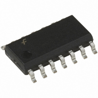
IC SWITCH BILATERAL QUAD 14-SOIC
Manufacturer
Fairchild Semiconductor
Series
4000Br
Type
Bilateral, FET Switchesr
Datasheet
1.CD4016BCM.pdf
(9 pages)
Specifications of CD4016BCM
Circuit
1 x 1:1
Independent Circuits
4
Voltage Supply Source
Dual Supply
Voltage - Supply
3 V ~ 15 V
Operating Temperature
-55°C ~ 125°C
Mounting Type
Surface Mount
Package / Case
14-SOIC (3.9mm Width), 14-SOL
Switch Configuration
SPST
On Resistance (max)
2000 Ohms
On Time (max)
50 ns
Off Time (max)
40 ns
Supply Voltage (max)
15 V
Supply Voltage (min)
3 V
Maximum Power Dissipation
500 mW
Maximum Operating Temperature
+ 125 C
Mounting Style
SMD/SMT
Minimum Operating Temperature
- 55 C
Propagation Delay Time
100 ns
Analog Switch Type
SPST
No. Of Channels
4
Bandwidth
40MHz
On State Resistance Max
850ohm
Turn Off Time
10ns
Turn On Time
17ns
Supply Voltage Range
3V To 15V
Rohs Compliant
Yes
Lead Free Status / RoHS Status
Contains lead / RoHS non-compliant
Current - Output High, Low
-
Lead Free Status / Rohs Status
Lead free / RoHS Compliant
Available stocks
Company
Part Number
Manufacturer
Quantity
Price
Company:

Part Number:
CD4016BCM
Manufacturer:
SAMSUNG
Quantity:
5
Part Number:
CD4016BCMX
Manufacturer:
FAIRCHILD/仙童
Quantity:
20 000


t
t
t
C
C
C
C
PHL
PZH
PHZ
AC Electrical Characteristics
T
Note 4: AC Parameters are guaranteed by DC correlated testing.
Note 5: These devices should not be connected to circuits with the power “ON”.
Note 6: In all cases, there is approximately 5 pF of probe and jig capacitance on the output; however, this capacitance is included in C
specified.
Note 7: V
IS
OS
IOS
IN
Symbol
A
, t
, t
, t
PLH
PZL
PLZ
25 C, t
IS
is the voltage at the in/out pin and V
Propagation Delay Time
Signal Input to Signal Output
Propagation Delay Time
Control Input to Signal
Output HIGH Impedance to
Logical Level
Propagation Delay Time
Control Input to Signal
Output Logical Level to
HIGH Impedance
Sine Wave Distortion
Frequency Response — Switch
“ON” (Frequency at 3 dB)
Feedthrough — Switch “OFF”
(Frequency at 50 dB)
Crosstalk Between Any Two
Switches (Frequency at 50 dB)
Crosstalk; Control Input to
Signal Output
Maximum Control Input
Signal Input Capacitance
Signal Output Capacitance
Feedthrough Capacitance
Control Input Capacitance
r
t
f
20 ns and V
Parameter
SS
0V unless otherwise specified
OS
is the voltage at the out/in pin. V
V
R
V
V
V
R
V
V
V
R
V
V
V
V
R
(Figure 4)
V
R
20 Log
(Figure 4)
V
R
20 Log
(Figure 4)
V
R
20 Log
(Figure 5)
V
R
C
R
V
V
V
V
V
V
C
DD
DD
DD
DD
DD
DD
DD
DD
DD
C
C
DD
DD
DD
OS(f)
DD
DD
DD
DD
C
(Note 4)
L
L
L
L
L
L
L
IN
L
L
200k
1.0 k , C
1.0 k , C
10 k , V
1 k , V
1 k , V
1 k V
50 pF (Figure 6)
1 k , C
V
V
V
0V
1 k , V
10V
5V
15V
5V
10V
15V
5V
10V
15V
5V, V
V
10V, R
5V
10V
15V
10V
DD
DD
DD
10
10
10
C(A)
½ V
, C
V
(V
(V
OS
IS(A)
5V, V
5V, V
C
OS
OS(B)
L
OS
IS
IS
L
L
CC
IS
/V
5V; V
3
L
L
/V
(1 kHz)
50 pF, (Figure 1)
V
OS
50 pF, (Figure 7)
5 V
5 V
IS
10 k
Conditions
/V
SS
SS
SS
5 V
5 V
50 pF, (Figure 2, Figure 3)
50 pF, (Figure 2, Figure 3)
)
10V Square Wave,
(1 kHz) dB,
OS(A)
C
SS
P-P
P-P
is the voltage at the control input.
P-P
P-P
50 dB,
5
5V,
,
5V,
,
,
)
, f
V
C(B)
1 kHz,
50 dB,
5V,
Min
1.25
Typ
150
0.4
6.5
8.0
9.0
0.2
0.9
58
27
20
20
18
17
15
11
10
40
4
4
5
www.fairchildsemi.com
L
wherever it is
Max
100
7.5
50
40
50
40
35
40
25
22
mV
Units
MHz
MHz
MHz
MHz
MHz
MHz
ns
ns
ns
ns
ns
ns
ns
ns
ns
pF
pF
pF
pF
%
P-P
Related parts for CD4016BCM
Image
Part Number
Description
Manufacturer
Datasheet
Request
R

Part Number:
Description:
Fairchild Semiconductor [IGBT MODULE]
Manufacturer:
Fairchild Semiconductor
Datasheet:

Part Number:
Description:
Discrete Semiconductor Modules
Manufacturer:
Fairchild Semiconductor
Part Number:
Description:
Discrete Semiconductor Modules
Manufacturer:
Fairchild Semiconductor
Part Number:
Description:
This N-Channel MOSFET is produced using Fairchild Semiconductor’s advanced Power Trench® process
Manufacturer:
Fairchild Semiconductor
Datasheet:
Part Number:
Description:
This N-Channel MOSFET is produced using Fairchild Semiconductor’s advanced Power Trench® process
Manufacturer:
Fairchild Semiconductor
Datasheet:
Part Number:
Description:
This N-Channel MOSFET is produced using Fairchild Semiconductor’s advanced PowerTrench® process
Manufacturer:
Fairchild Semiconductor
Datasheet:
Part Number:
Description:
This N-Channel MOSFET is produced using Fairchild Semiconductor’s advanced PowerTrench® process
Manufacturer:
Fairchild Semiconductor
Datasheet:
Part Number:
Description:
This N-Channel MOSFET is produced using Fairchild Semiconductor’s advanced Power Trench® process
Manufacturer:
Fairchild Semiconductor
Datasheet:
Part Number:
Description:
This N-Channel logic Level MOSFETs are produced using Fairchild Semiconductor‘s advanced Power Trench® process that has been special tailored to minimize the on-state resistance and yet maintain superior switching performance
Manufacturer:
Fairchild Semiconductor
Datasheet:
Part Number:
Description:
This N-Channel MOSFET is produced using Fairchild Semiconductor’s advanced Power Trench® process
Manufacturer:
Fairchild Semiconductor
Datasheet:
Part Number:
Description:
This N-Channel SyncFET™ is produced using Fairchild Semiconductor’s advanced PowerTrench® process
Manufacturer:
Fairchild Semiconductor
Datasheet:
Part Number:
Description:
This N-Channel SyncFET™ is produced using Fairchild Semiconductor’s advanced PowerTrench® process
Manufacturer:
Fairchild Semiconductor
Datasheet:
Part Number:
Description:
This N-Channel SyncFET™ is produced using Fairchild Semiconductor’s advanced PowerTrench® process
Manufacturer:
Fairchild Semiconductor
Datasheet:
Part Number:
Description:
This N-Channel logic Level MOSFETs are produced using Fairchild Semiconductor‘s advanced Power Trench® process that has been special tailored to minimize the on-state resistance and yet maintain superior switching performance
Manufacturer:
Fairchild Semiconductor
Datasheet:
Part Number:
Description:
This N-Channel MOSFET is produced using Fairchild Semiconductor’s advanced Power Trench® process that has been especially tailored to minimize the on-state resistance and yet maintain superior switching performance
Manufacturer:
Fairchild Semiconductor
Datasheet: