CD4094BCN Fairchild Semiconductor, CD4094BCN Datasheet
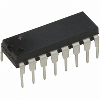
IC REGISTER/LATCH 8BIT 3ST 16DIP

CD4094BCN

Manufacturer Part Number
CD4094BCN
Description
IC REGISTER/LATCH 8BIT 3ST 16DIP
Manufacturer
Fairchild Semiconductor
Series
4000Br
Datasheet

Specifications of CD4094BCN

Logic Type
Shift Register
Output Type
Standard
Number Of Elements
1
Number Of Bits Per Element
8
Function
Serial to Parallel
Voltage - Supply
3 V ~ 18 V
Operating Temperature
-40°C ~ 85°C
Mounting Type
Through Hole
Package / Case
16-DIP (0.300", 7.62mm)
Lead Free Status / RoHS Status
Lead free / RoHS Compliant
Other names
4094

Available stocks

Company
Part Number
Manufacturer
Quantity
Price
Part Number:
CD4094BCN
Quantity:
219
Part Number:
CD4094BCN
Manufacturer:
HAR
Quantity:
8
Part Number:
CD4094BCN
Manufacturer:
FAIRCHILD/仙童
Quantity:
20 000
© 1999 Fairchild Semiconductor Corporation
CD4094BCWM
CD4094BCN
CD4094BC
8-Bit Shift Register/Latch with 3-STATE Outputs
General Description
The CD4094BC consists of an 8-bit shift register and a 3-
STATE 8-bit latch. Data is shifted serially through the shift
register on the positive transition of the clock. The output of
the last stage (Q
devices. Data on the Q
output, Q
The output of each stage of the shift register feeds a latch,
which latches data on the negative edge of the STROBE
input. When STROBE is HIGH, data propagates through
Ordering Code:
Devices also available in Tape and Reel. Specify by appending the suffix letter “X” to the ordering code.
Connection Diagram
Truth Table

X

Note 1: At the positive clock edge, information in the 7th shift register stage is transferred to Q8 and Q
Order Number
Don't Care
HIGH-to-LOW
LOW-to-HIGH
S
, on the following negative clock edge.
Clock


Package Number
S
) can be used to cascade several
S
M16B
N16E
output is transferred to a second
Output
Enable
0
0
1
1
1
1
16-Lead Small Outline Integrated Circuit (SOIC), JEDEC MS-013, 0.300” Wide
16-Lead Plastic Dual-In-Line Package (PDIP), JEDEC MS-001, 0.300” Wide
Strobe
X
X
0
1
1
1
Pin Assignments for DIP and SOIC
DS005983.prf
Data
X
X
X
0
1
1
Top View
No Change No Change
No Change No Change No Change
Parallel Outputs
Hi-Z
Hi-Z
the latch to 3-STATE output gates. These gates are
enabled when OUTPUT ENABLE is taken HIGH.
Features
Q1
0
1
Wide supply voltage range:
High noise immunity: 0.45 V
Low power TTL compatibility:
3-STATE outputs
Fan out of 2 driving 74L or 1 driving 74LS
Package Description
Q
Q
Hi-Z
Hi-Z
Q
N
N
N
1
1
S
.
No Change
(Note 1)
Q
Q7
Q7
Q7
Q7
Serial Outputs
S
October 1987
Revised January 1999
DD
3.0V to 18V
No Change
No Change
No Change
No Change
(typ.)
Q
Q7
Q7
www.fairchildsemi.com

Related parts for CD4094BCN

CD4094BCN Summary of contents

Page 1

... CD4094BCWM M16B 16-Lead Small Outline Integrated Circuit (SOIC), JEDEC MS-013, 0.300” Wide CD4094BCN N16E 16-Lead Plastic Dual-In-Line Package (PDIP), JEDEC MS-001, 0.300” Wide Devices also available in Tape and Reel. Specify by appending the suffix letter “X” to the ordering code. ...

Page 2

Block Diagram www.fairchildsemi.com 2 ...

Page 3

Absolute Maximum Ratings (Note 3) Supply Voltage ( Input Voltage ( Storage Temperature Range ( Power Dissipation ( Dual-In-Line Small Outline ) Lead Temperature (T L (Soldering, 10 seconds) ...

Page 4

AC Electrical Characteristics Symbol Parameter Propagation Delay PHL PLH Clock Propagation Delay PHL PLH Clock Propagation Delay Clock ...

Page 5

Timing Diagram Test Circuits and Timing Diagrams for 3-STATE 5 www.fairchildsemi.com ...

Page 6

Physical Dimensions inches (millimeters) unless otherwise noted 16-Lead Small Outline Integrated Circuit (SOIC), JEDEC MS-013, 0.300” Wide www.fairchildsemi.com M16B 6 ...

Page 7

Physical Dimensions inches (millimeters) unless otherwise noted (Continued) 16-Lead Plastic Dual-In-Line Package (PDIP), JEDEC MS-001, 0.300” Wide LIFE SUPPORT POLICY FAIRCHILD’S PRODUCTS ARE NOT AUTHORIZED FOR USE AS CRITICAL COMPONENTS IN LIFE SUPPORT DEVICES OR SYSTEMS WITHOUT THE EXPRESS WRITTEN ...

Related keywords