CD4538BCN Fairchild Semiconductor, CD4538BCN Datasheet
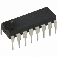
IC MULTIVIBRATOR MONO DUAL 16DIP

CD4538BCN

Manufacturer Part Number
CD4538BCN
Description
IC MULTIVIBRATOR MONO DUAL 16DIP
Manufacturer
Fairchild Semiconductor
Series
4000Br
Datasheet

Specifications of CD4538BCN

Logic Type
Monostable
Independent Circuits
2
Schmitt Trigger Input
No
Propagation Delay
100ns
Current - Output High, Low
8.8mA, 8.8mA
Voltage - Supply
3 V ~ 15 V
Operating Temperature
-55°C ~ 125°C
Mounting Type
Through Hole
Package / Case
16-DIP (0.300", 7.62mm)
Elements Per Chip
2
Logic Family
CD4000
Input Bias Current (max)
0.02 mA
Propagation Delay Time
600 ns, 300 ns, 220 ns
High Level Output Current
- 4.2 mA
Low Level Output Current
4.2 mA
Supply Voltage (max)
15 V
Supply Voltage (min)
3 V
Maximum Operating Temperature
+ 125 C
Minimum Operating Temperature
- 55 C
Mounting Style
Through Hole
Operating Supply Voltage
3.3 V, 5 V, 9 V, 12 V
Lead Free Status / RoHS Status
Lead free / RoHS Compliant

Available stocks

Company
Part Number
Manufacturer
Quantity
Price
Part Number:
CD4538BCN
Manufacturer:
MOT
Quantity:
512
Part Number:
CD4538BCN
Manufacturer:
FSC大量供
Quantity:
20 000
© 1999 Fairchild Semiconductor Corporation
CD4538BCM
CD4538BCWM
CD4538BCN
CD4538BC
Dual Precision Monostable
General Description
The CD4538BC is a dual, precision monostable multivibra-
tor with independent trigger and reset controls. The device
is retriggerable and resettable, and the control inputs are
internally latched. Two trigger inputs are provided to allow
either rising or falling edge triggering. The reset inputs are
active LOW and prevent triggering while active. Precise
control of output pulse-width has been achieved using lin-
ear CMOS techniques. The pulse duration and accuracy
are determined by external components R
device does not allow the timing capacitor to discharge
through the timing pin on power-down condition. For this
reason, no external protection resistor is required in series
with the timing pin. Input protection from static discharge is
provided on all pins.
Ordering Code:
Devices also available in Tape and Reel. Specify by appending the suffix letter “X” to the ordering code.
Connection Diagram
Order Number
Pin Assignments for DIP and SOIC
Package Number
Top View
M16A
M16B
N16E
16-Lead Small Outline Integrated Circuit (SOIC), JEDEC MS-012, 0.150” Narrow Body
16-Lead Small Outline Integrated Circuit (SOIC), JEDEC MS-013, 0.300” Wide Body
16-Lead Plastic Dual-In-Line Package (PDIP), JEDEC MS-001, 0.300” Wide
X
DS006000.prf
and C
X
. The
Features
Truth Table
H
L
X
Wide supply voltage range:
High noise immunity: 0.45 V
Low power TTL compatibility: Fan out of 2 driving 74L
or 1 driving 74LS
New formula: PW
C in Farads)
Wide pulse-width range: 1 s to
Separate latched reset inputs
Symmetrical output sink and source capability
Low standby current: 5 nA (typ.) @ 5 V
Pin compatible to CD4528BC
LOW Level
Transition from LOW-to-HIGH
Transition from HIGH-to-LOW
Irrelevant
HIGH Level
1.0% pulse-width variation from part to part (typ.)
One HIGH Level Pulse
One LOW Level Pulse
Package Description
Clear
H
H
X
X
L
Inputs
OUT
A
X
H
X
L
RC (PW in seconds, R in Ohms,
October 1987
Revised January 1999
B
X
X
H
L
CC
3.0V to 15V
(typ.)
Q
L
L
L
Outputs
www.fairchildsemi.com
DC
Q
H
H
H

Related parts for CD4538BCN

CD4538BCN Summary of contents

Page 1

... CD4538BCWM M16B 16-Lead Small Outline Integrated Circuit (SOIC), JEDEC MS-013, 0.300” Wide Body CD4538BCN N16E 16-Lead Plastic Dual-In-Line Package (PDIP), JEDEC MS-001, 0.300” Wide Devices also available in Tape and Reel. Specify by appending the suffix letter “X” to the ordering code. ...

Page 2

Block Diagram R and C are External Components Pin Pin 8 SS Logic Diagram www.fairchildsemi.com FIGURE 1. 2 ...

Page 3

Theory of Operation Trigger Operation The block diagram of the CD4538BC is shown in Figure 1, with circuit operation following. As shown in Figure 1 and Figure 2, before an input trigger occurs, the monostable is in the quiescent state ...

Page 4

FIGURE 3. Retriggerable Monostables Circuitry FIGURE 5. Connection of Unused Sections www.fairchildsemi.com FIGURE 4. Non-Retriggerable Monostables Circuitry 4 ...

Page 5

Absolute Maximum Ratings (Note 2) DC Supply Voltage ( Input Voltage ( Storage Temperature Range ( Power Dissipation ( Dual-In-Line Small Outline ) Lead Temperature (T L (Soldering, 10 ...

Page 6

AC Electrical Characteristics pF, and unless otherwise specified Symbol Parameter Output Transition Time TLH THL Propagation Delay Time PLH PHL t ...

Page 7

Typical Applications FIGURE 6. Typical Normalized Distribution of Units for Output Pulse Width FIGURE 7. Typical Pulse Width Variation as a Function of Supply Voltage V FIGURE 8. Typical Total Supply Current Versus Output Duty Cycle, R 100 k , ...

Page 8

Test Circuits and Waveforms FIGURE 12. Switching Test Waveforms * PLH PW OUT PLH PW OUT t PLH( *Includes capacitance of probes, wiring, and fixture parasitic Note: ...

Page 9

R R 100 100 0 Duty Cycle 50% FIGURE 14. Power Dissipation Test Circuit and Waveforms 9 www.fairchildsemi.com ...

Page 10

Physical Dimensions inches (millimeters) unless otherwise noted 16-Lead Small Outline Integrated Circuit (SOIC), JEDEC MS-012, 0.150” Narrow Body 16-Lead Small Outline Integrated Circuit (SOIC), JEDEC MS-013, 0.300” Wide Body www.fairchildsemi.com Package Number M16A Package Number M16B 10 ...

Page 11

Physical Dimensions inches (millimeters) unless otherwise noted (Continued) 16-Lead Plastic Dual-In-Line Package (PDIP), JEDEC MS-001, 0.300” Wide LIFE SUPPORT POLICY FAIRCHILD’S PRODUCTS ARE NOT AUTHORIZED FOR USE AS CRITICAL COMPONENTS IN LIFE SUPPORT DEVICES OR SYSTEMS WITHOUT THE EXPRESS WRITTEN ...

Related keywords