MM74HC259MTC Fairchild Semiconductor, MM74HC259MTC Datasheet - Page 3
MM74HC259MTC
Manufacturer Part Number
MM74HC259MTC
Description
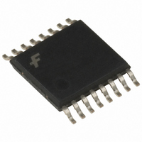
IC DCDR/3:8L LATCH 8BIT 16-TSSOP
Manufacturer
Fairchild Semiconductor
Series
74HCr
Type
D-Typer
Datasheet
1.MM74HC259MTC.pdf
(7 pages)
Specifications of MM74HC259MTC
Logic Type
D-Type, Addressable
Circuit
1:8
Output Type
Standard
Voltage - Supply
2 V ~ 6 V
Independent Circuits
1
Delay Time - Propagation
17ns
Current - Output High, Low
5.2mA, 5.2mA
Operating Temperature
-40°C ~ 85°C
Mounting Type
Surface Mount
Package / Case
16-TSSOP
Logic Family
HC
Number Of Bits
8
Number Of Elements
1
Latch Mode
Addressable
Polarity
Non-Inverting
Technology
CMOS
Package Type
TSSOP
Propagation Delay Time
275ns
Operating Supply Voltage (typ)
2.5/3.3/5V
High Level Output Current
-5.2mA
Low Level Output Current
5.2mA
Operating Supply Voltage (min)
2V
Operating Supply Voltage (max)
6V
Operating Temp Range
-40C to 85C
Operating Temperature Classification
Industrial
Mounting
Surface Mount
Pin Count
16
Lead Free Status / RoHS Status
Lead free / RoHS Compliant


V
V
V
V
I
I
IN
CC
Supply Voltage (V
DC Input Voltage (V
DC Output Voltage (V
Clamp Diode Current (I
DC Output Current, per pin (I
DC V
Storage Temperature Range (T
Power Dissipation (P
Lead Temperature (T
Symbol
Absolute Maximum Ratings
(Note 2)
DC Electrical Characteristics
IH
IL
OH
OL
Note 4: For a power supply of 5V 10% the worst case output voltages (V
designing with this supply. Worst case V
(I
IN
(Note 3)
S.O. Package only
(Soldering 10 seconds)
, I
CC
CC
, and I
or GND Current, per pin (I
Minimum HIGH Level
Input Voltage
Maximum LOW Level
Input Voltage
Minimum HIGH Level
Output Voltage
Maximum LOW Level
Output Voltage
Maximum Input
Current
Maximum Quiescent
Supply Current
OZ
) occur for CMOS at the higher voltage and so the 6.0V values should be used.
Parameter
CC
IN
)
D
L
)
OUT
)
)
IK
, I
)
OK
OUT
)
V
|I
V
|I
|I
V
|I
V
|I
|I
V
V
I
STG
OUT
IH
OUT
OUT
OUT
OUT
OUT
OUT
IN
IN
IN
IN
IN
IN
)
and V
CC
)
|
|
|
|
|
|
Conditions
V
V
V
V
V
V
0 A
IH
IH
IH
IH
CC
CC
)
20 A
4.0 mA
5.2 mA
20 A
4.0 mA
5.2 mA
IL
or V
or V
or V
or V
or GND
or GND
occur at V
IL
IL
IL
IL
1.5 to V
0.5 to V
65 C to 150 C
(Note 1)
CC
0.5 to 7.0V
5.5V and 4.5V respectively. (The V
(Note 4)
CC
CC
600 mW
500 mW
2.0V
4.5V
6.0V
2.0V
4.5V
6.0V
2.0V
4.5V
6.0V
4.5V
6.0V
2.0V
4.5V
6.0V
4.5V
6.0V
6.0V
6.0V
V
20 mA
25 mA
50 mA
260 C
CC
1.5V
0.5V
OH
, and V
3
Recommended Operating
Conditions
Note 1: Absolute Maximum Ratings are those values beyond which dam-
age to the device may occur.
Note 2: Unless otherwise specified all voltages are referenced to ground.
Note 3: Power Dissipation temperature derating — plastic “N” package:
12 mW/ C from 65 C to 85 C
Supply Voltage (V
DC Input or Output Voltage
Operating Temperature Range (T
Input Rise or Fall Times
Typ
2.0
4.5
6.0
4.2
5.7
0.2
0.2
0
0
0
(V
(t
OL
T
r
IN
A
, t
) occur for HC at 4.5V. Thus the 4.5V values should be used when
, V
f
) V
25 C
V
V
OUT
CC
CC
CC
3.15
1.35
3.98
5.48
0.26
0.26
1.5
4.2
0.5
1.8
1.9
4.4
5.9
0.1
0.1
0.1
8.0
0.1
)
IH
2.0V
4.5V
6.0V
value at 5.5V is 3.85V.) The worst case leakage current
CC
T
A
)
Guaranteed Limits
40 to 85 C T
3.15
1.35
3.84
5.34
0.33
0.33
1.5
4.2
0.5
1.8
1.9
4.4
5.9
0.1
0.1
0.1
80
1.0
A
)
A
Min
40
2
0
www.fairchildsemi.com
55 to 125 C
3.15
1.35
160
1.5
4.2
0.5
1.8
1.9
4.4
5.9
3.7
5.2
0.1
0.1
0.1
0.4
0.4
1.0
1000
Max
V
500
400
6
CC
85
Units
Units
ns
ns
ns
V
V
C
V
V
V
V
V
V
V
V
V
V
V
V
V
V
V
V
A
A
Related parts for MM74HC259MTC
Image
Part Number
Description
Manufacturer
Datasheet
Request
R

Part Number:
Description:
Fairchild Semiconductor [IGBT MODULE]
Manufacturer:
Fairchild Semiconductor
Datasheet:

Part Number:
Description:
Discrete Semiconductor Modules
Manufacturer:
Fairchild Semiconductor
Part Number:
Description:
Discrete Semiconductor Modules
Manufacturer:
Fairchild Semiconductor
Part Number:
Description:
This N-Channel MOSFET is produced using Fairchild Semiconductor’s advanced Power Trench® process
Manufacturer:
Fairchild Semiconductor
Datasheet:
Part Number:
Description:
This N-Channel MOSFET is produced using Fairchild Semiconductor’s advanced Power Trench® process
Manufacturer:
Fairchild Semiconductor
Datasheet:
Part Number:
Description:
This N-Channel MOSFET is produced using Fairchild Semiconductor’s advanced PowerTrench® process
Manufacturer:
Fairchild Semiconductor
Datasheet:
Part Number:
Description:
This N-Channel MOSFET is produced using Fairchild Semiconductor’s advanced PowerTrench® process
Manufacturer:
Fairchild Semiconductor
Datasheet:
Part Number:
Description:
This N-Channel MOSFET is produced using Fairchild Semiconductor’s advanced Power Trench® process
Manufacturer:
Fairchild Semiconductor
Datasheet:
Part Number:
Description:
This N-Channel logic Level MOSFETs are produced using Fairchild Semiconductor‘s advanced Power Trench® process that has been special tailored to minimize the on-state resistance and yet maintain superior switching performance
Manufacturer:
Fairchild Semiconductor
Datasheet:
Part Number:
Description:
This N-Channel MOSFET is produced using Fairchild Semiconductor’s advanced Power Trench® process
Manufacturer:
Fairchild Semiconductor
Datasheet:
Part Number:
Description:
This N-Channel SyncFET™ is produced using Fairchild Semiconductor’s advanced PowerTrench® process
Manufacturer:
Fairchild Semiconductor
Datasheet:
Part Number:
Description:
This N-Channel SyncFET™ is produced using Fairchild Semiconductor’s advanced PowerTrench® process
Manufacturer:
Fairchild Semiconductor
Datasheet:
Part Number:
Description:
This N-Channel SyncFET™ is produced using Fairchild Semiconductor’s advanced PowerTrench® process
Manufacturer:
Fairchild Semiconductor
Datasheet:
Part Number:
Description:
This N-Channel logic Level MOSFETs are produced using Fairchild Semiconductor‘s advanced Power Trench® process that has been special tailored to minimize the on-state resistance and yet maintain superior switching performance
Manufacturer:
Fairchild Semiconductor
Datasheet:
Part Number:
Description:
This N-Channel MOSFET is produced using Fairchild Semiconductor’s advanced Power Trench® process that has been especially tailored to minimize the on-state resistance and yet maintain superior switching performance
Manufacturer:
Fairchild Semiconductor
Datasheet: