74LCX373MTC Fairchild Semiconductor, 74LCX373MTC Datasheet - Page 2
74LCX373MTC
Manufacturer Part Number
74LCX373MTC
Description
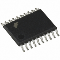
IC LATCH TRANSP OCT LV 20-TSSOP
Manufacturer
Fairchild Semiconductor
Series
74LCXr
Type
D-Typer
Datasheet
1.74LCX373MTC.pdf
(15 pages)
Specifications of 74LCX373MTC
Logic Type
D-Type Transparent Latch
Circuit
8:8
Output Type
Tri-State
Voltage - Supply
2 V ~ 3.6 V
Independent Circuits
1
Delay Time - Propagation
1.5ns
Current - Output High, Low
24mA, 24mA
Operating Temperature
-40°C ~ 85°C
Mounting Type
Surface Mount
Package / Case
20-TSSOP
Logic Family
LCX
Number Of Bits
8
Number Of Elements
1
Latch Mode
Transparent
Polarity
Non-Inverting
Technology
CMOS
Package Type
TSSOP
Propagation Delay Time
10.5ns
Operating Supply Voltage (typ)
2.5/3.3V
High Level Output Current
-24mA
Low Level Output Current
24mA
Operating Supply Voltage (min)
2V
Operating Supply Voltage (max)
3.6V
Operating Temp Range
-40C to 85C
Operating Temperature Classification
Industrial
Mounting
Surface Mount
Pin Count
20
Lead Free Status / RoHS Status
Lead free / RoHS Compliant
Available stocks
Company
Part Number
Manufacturer
Quantity
Price

Part Number:
74LCX373MTCX
Manufacturer:
FAIRCHILD/仙童
Quantity:
20 000


©2006 Fairchild Semiconductor Corporation
74LCX373 Rev. 1.8.0
Connection Diagrams
Pin Descriptions
D
LE
OE
O
Pin Names
0
0
–D
–O
7
7
Pad Assignments for DQFN
SOIC, SOP, SSOP, TSSOP
GND
OE
O
D
D
O
O
D
D
O
Pin Assignments for
O
O
O
O
D
D
D
D
Data Inputs
Latch Enable Input
3-STATE Output Enable Input
3-STATE Latch Outputs
0
0
1
1
2
2
3
3
0
0
1
1
2
2
3
3
2
3
4
5
6
7
8
9
1
2
3
4
5
6
7
8
9
10
(Top View)
GND
OE
10
1
V
LE
11
20
Description
CC
20
19
18
17
16
15
14
13
12
11
19
18
17
16
15
14
13
12
O
D
D
O
O
D
D
O
7
7
6
6
5
5
4
4
V
O
D
D
O
O
D
D
O
LE
CC
7
7
6
6
5
5
4
4
2
Logic Symbols
Truth Table
H = HIGH Voltage
L = LOW Voltage
Z = High Impedance
X = Immaterial
O
of Latch Enable
Functional Description
The LCX373 contains eight D-type latches with 3-STATE
standard outputs. When the Latch Enable (LE) input is
HIGH, data on the D
condition the latches are transparent, i.e. a latch output
will change state each time its D input changes. When
LE is LOW, the latches store the information that was
present on the D inputs a setup time preceding the
HIGH-to-LOW transition of LE. The 3-STATE standard
outputs are controlled by the Output Enable (OE) input.
When OE is LOW, the standard outputs are in the
2-state mode. When OE is HIGH, the standard outputs
are in the high impedance mode but this does not inter-
fere with entering new data into the latches.
0
= Previous O
LE
H
H
X
L
Inputs
OE
LE
D
D
D
D
D
D
D
D
0
OE
LE
0
1
2
3
4
5
6
7
OE
before HIGH-to-LOW transition
H
L
L
L
D
O
0
0
n
O
D
EN
C1
1D
1
1
inputs enters the latches. In this
O
D
IEEE/IEC
2
2
D
O
3
3
D
O
D
H
X
X
4
L
4
n
D
O
5
5
O
D
6
6
O
D
O
O
O
O
O
O
O
O
7
7
0
1
2
3
4
5
6
7
Outputs
www.fairchildsemi.com
O
O
H
Z
L
n
0
Related parts for 74LCX373MTC
Image
Part Number
Description
Manufacturer
Datasheet
Request
R

Part Number:
Description:
Fairchild Semiconductor [IGBT MODULE]
Manufacturer:
Fairchild Semiconductor
Datasheet:

Part Number:
Description:
Discrete Semiconductor Modules
Manufacturer:
Fairchild Semiconductor
Part Number:
Description:
Discrete Semiconductor Modules
Manufacturer:
Fairchild Semiconductor
Part Number:
Description:
This N-Channel MOSFET is produced using Fairchild Semiconductor’s advanced Power Trench® process
Manufacturer:
Fairchild Semiconductor
Datasheet:
Part Number:
Description:
This N-Channel MOSFET is produced using Fairchild Semiconductor’s advanced Power Trench® process
Manufacturer:
Fairchild Semiconductor
Datasheet:
Part Number:
Description:
This N-Channel MOSFET is produced using Fairchild Semiconductor’s advanced PowerTrench® process
Manufacturer:
Fairchild Semiconductor
Datasheet:
Part Number:
Description:
This N-Channel MOSFET is produced using Fairchild Semiconductor’s advanced PowerTrench® process
Manufacturer:
Fairchild Semiconductor
Datasheet:
Part Number:
Description:
This N-Channel MOSFET is produced using Fairchild Semiconductor’s advanced Power Trench® process
Manufacturer:
Fairchild Semiconductor
Datasheet:
Part Number:
Description:
This N-Channel logic Level MOSFETs are produced using Fairchild Semiconductor‘s advanced Power Trench® process that has been special tailored to minimize the on-state resistance and yet maintain superior switching performance
Manufacturer:
Fairchild Semiconductor
Datasheet:
Part Number:
Description:
This N-Channel MOSFET is produced using Fairchild Semiconductor’s advanced Power Trench® process
Manufacturer:
Fairchild Semiconductor
Datasheet:
Part Number:
Description:
This N-Channel SyncFET™ is produced using Fairchild Semiconductor’s advanced PowerTrench® process
Manufacturer:
Fairchild Semiconductor
Datasheet:
Part Number:
Description:
This N-Channel SyncFET™ is produced using Fairchild Semiconductor’s advanced PowerTrench® process
Manufacturer:
Fairchild Semiconductor
Datasheet:
Part Number:
Description:
This N-Channel SyncFET™ is produced using Fairchild Semiconductor’s advanced PowerTrench® process
Manufacturer:
Fairchild Semiconductor
Datasheet:
Part Number:
Description:
This N-Channel logic Level MOSFETs are produced using Fairchild Semiconductor‘s advanced Power Trench® process that has been special tailored to minimize the on-state resistance and yet maintain superior switching performance
Manufacturer:
Fairchild Semiconductor
Datasheet:
Part Number:
Description:
This N-Channel MOSFET is produced using Fairchild Semiconductor’s advanced Power Trench® process that has been especially tailored to minimize the on-state resistance and yet maintain superior switching performance
Manufacturer:
Fairchild Semiconductor
Datasheet: