DM7473N Fairchild Semiconductor, DM7473N Datasheet
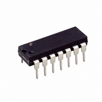
IC F/F DUAL POS TRIG JK 14-DIP

DM7473N

Manufacturer Part Number
DM7473N
Description
IC F/F DUAL POS TRIG JK 14-DIP
Manufacturer
Fairchild Semiconductor
Series
7400r
Type
JK Typer
Datasheet

Specifications of DM7473N

Function
Set(Preset) and Reset
Output Type
Differential
Number Of Elements
2
Number Of Bits Per Element
1
Frequency - Clock
15MHz
Delay Time - Propagation
25ns
Trigger Type
Positive Edge
Current - Output High, Low
400µA, 16mA
Voltage - Supply
4.75 V ~ 5.25 V
Operating Temperature
0°C ~ 70°C
Mounting Type
Through Hole
Package / Case
14-DIP (0.300", 7.62mm)
Lead Free Status / RoHS Status
Lead free / RoHS Compliant
Other names
7473
7473N

Available stocks

Company
Part Number
Manufacturer
Quantity
Price
Part Number:
DM7473N
Quantity:
1
Part Number:
DM7473N
Manufacturer:
MICROCHIP
Quantity:
30
© 2001 Fairchild Semiconductor Corporation
DM7473N
DM7473
Dual Master-Slave J-K Flip-Flops
with Clear and Complementary Outputs
General Description
This device contains two independent positive pulse trig-
gered J-K flip-flops with complementary outputs. The J and
K data is processed by the flip-flops after a complete clock
pulse. While the clock is LOW the slave is isolated from the
master. On the positive transition of the clock, the data
from the J and K inputs is transferred to the master. While
the clock is HIGH the J and K inputs are disabled. On the
Ordering Code:
Connection Diagram
Order Number
Package Number
N14A
14-Lead Plastic Dual-In-Line Package (PDIP), JEDEC MS-001, 0.300" Wide
DS006525
negative transition of the clock, the data from the master is
transferred to the slave. The logic states of the J and K
inputs must not be allowed to change while the clock is
HIGH. Data transfers to the outputs on the falling edge of
the clock pulse. A LOW logic level on the clear input will
reset the outputs regardless of the logic states of the other
inputs.
Function Table
H
L
X
Q
Toggle
0
LOW Logic Level
Either LOW or HIGH Logic Level
HIGH Logic Level
CLR
the clock is HIGH. Data is transferred to the outputs on the falling
edge of the clock pulse.
established.
each HIGH level clock pulse.
Positive pulse data. the J and K inputs must be held constant while
The output logic level before the indicated input conditions were
H
H
H
H
L
Package Description
Each output changes to the complement of its previous level on
CLK
X
Inputs
H
H
X
J
L
L
September 1986
Revised July 2001
K
X
H
H
L
L
www.fairchildsemi.com
Q
Q
H
L
L
0
Outputs
Toggle
Q
Q
H
H
L
0

Related parts for DM7473N

DM7473N Summary of contents

Page 1

... J and K inputs is transferred to the master. While the clock is HIGH the J and K inputs are disabled. On the Ordering Code: Order Number Package Number DM7473N N14A 14-Lead Plastic Dual-In-Line Package (PDIP), JEDEC MS-001, 0.300" Wide Connection Diagram © 2001 Fairchild Semiconductor Corporation negative transition of the clock, the data from the master is transferred to the slave ...

Page 2

Absolute Maximum Ratings Supply Voltage Input Voltage Operating Free Air Temperature Range Storage Temperature Range Recommended Operating Conditions Symbol Parameter V Supply Voltage CC V HIGH Level Input Voltage IH V LOW Level Input Voltage IL I HIGH Level Output ...

Page 3

Physical Dimensions inches (millimeters) unless otherwise noted 14-Lead Plastic Dual-In-Line Package (PDIP), JEDEC MS-001, 0.300" Wide Fairchild does not assume any responsibility for use of any circuitry described, no circuit patent licenses are implied and Fairchild reserves the right at ...

Related keywords