MM74HC574MTCX Fairchild Semiconductor, MM74HC574MTCX Datasheet - Page 2
MM74HC574MTCX
Manufacturer Part Number
MM74HC574MTCX
Description
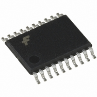
IC FLIP FLOP OCT D 3ST 20-TSSOP
Manufacturer
Fairchild Semiconductor
Series
74HCr
Type
D-Type Busr
Datasheet
1.MM74HC574WM.pdf
(8 pages)
Specifications of MM74HC574MTCX
Function
Standard
Output Type
Tri-State Non Inverted
Number Of Elements
1
Number Of Bits Per Element
8
Frequency - Clock
35MHz
Delay Time - Propagation
18ns
Trigger Type
Positive Edge
Current - Output High, Low
7.8mA, 7.8mA
Voltage - Supply
2 V ~ 6 V
Operating Temperature
-40°C ~ 85°C
Mounting Type
Surface Mount
Package / Case
20-TSSOP
Lead Free Status / RoHS Status
Lead free / RoHS Compliant


www.fairchildsemi.com
V
V
V
V
I
I
I
'
IN
OZ
CC
Symbol
Absolute Maximum Ratings
(Note 2)
DC Electrical Characteristics
Note 4: For a power supply of 5V
designing with this supply. Worst-case V
rent (I
I
IH
IL
OH
OL
Supply Voltage (V
DC Input Voltage (V
DC Output Voltage (V
Clamp Diode Current (I
DC Output Current, per pin (I
DC V
Storage Temperature Range (T
Power Dissipation (P
Lead Temperature (T
CC
(Note 3)
S.O. Package only
(Soldering 10 seconds)
IN
, I
CC
CC
Minimum HIGH Level Input
Voltage
Maximum LOW Level Input
Voltage
Minimum HIGH Level Output
Voltage
Maximum LOW Level Output
Voltage
Maximum Input Current
Maximum 3-STATE
Output Leakage Current
Maximum Quiescent Supply
Current
Quiescent Supply Current
per Input Pin
or GND Current, per pin (I
, and I
OZ
) occur for CMOS at the higher voltage and so the 6.0V values should be used.
Parameter
CC
IN
)
D
L
OUT
)
)
)
IK
, I
)
r
OK
10% the worst-case output voltages (V
OUT
)
IH
STG
)
and V
CC
)
)
V
|I
V
|I
|I
V
|I
V
|I
|I
V
V
OC
V
I
V
V
or 0.4V (Note 4)
IL
OUT
OUT
OUT
OUT
OUT
OUT
OUT
IN
IN
IN
IN
IN
OUT
IN
CC
IN
occur at V
Conditions
|
|
|
|
|
|
V
V
V
V
V
V
2.4V
V
1.5 to V
0.5 to V
d
d
d
d
d
d
5.5V
0
IH
IH
IH
IH
CC
CC
65
IH
V
20
6.0 mA
7.8 mA
20
6.0 mA
7.8 mA
P
CC
or V
or V
or V
or V
(Note 1)
A
q
or GND
or GND
C to
P
P
0.5 to
CC
A
A
or GND
IL
IL
IL
IL
(Note 4)
CC
CC
600 mW
500 mW
5.5V and 4.5V respectively. (The V
r
r
r
20 mA
35 mA
70 mA
150
260
7.0V
1.5V
0.5V
q
q
C
C
DATA
OH
2.0V
4.5V
6.0V
2.0V
4.5V
6.0V
2.0V
4.5V
6.0V
4.5V
6.0V
2.0V
4.5V
6.0V
4.5V
6.0V
6.0V
6.0V
6.0V
CLK
V
OE
CC
, and V
2
Supply Voltage (V
DC Input or Output Voltage
Operating Temperature Range (T
Input Rise or Fall Times
Recommended Operating
Conditions
Note 1: Maximum Ratings are those values beyond which damage to the
device may occur.
Note 2: Unless otherwise specified all voltages are referenced to ground.
Note 3: Power Dissipation temperature derating — plastic “N” package:
12 mW/
(V
(t
r
, t
OL
IN
f
,V
Typ
) occur for HC at 4.5V. Thus the 4.5V values should be used when
)
q
2.0
4.5
6.0
4.2
5.7
0.2
0.2
1.0
0.6
0.4
C from 65
0
0
0
OUT
T
A
V
V
V
)
CC
25
CC
CC
q
q
3.15
1.35
3.98
5.48
0.26
0.26
r
r
C
C to 85
1.5
4.2
0.5
1.8
1.9
4.4
5.9
0.1
0.1
0.1
8.0
1.5
0.8
0.5
IH
0.1
0.5
2.0V
4.5V
6.0V
CC
value at 5.5V is 3.85V.) The worst-case leakage cur-
)
q
C.
T
A
Guaranteed Limits
40 to 85
3.15
1.35
3.84
5.34
0.33
0.33
r
r
1.5
4.2
0.5
1.8
1.9
4.4
5.9
0.1
0.1
0.1
1.8
1.0
0.6
80
1.0
5.0
A
)
q
C T
Min
2
0
40
A
55 to 125
3.15
1.35
r
r
160
1.5
4.2
0.5
1.8
1.9
4.4
5.9
3.7
5.2
0.1
0.1
0.1
0.4
0.4
2.0
1.1
0.7
1000
Max
1.0
V
10
500
400
6
CC
85
q
C
Units
q
ns
ns
ns
V
V
Units
C
mA
P
P
P
V
V
V
V
V
V
A
A
A
Related parts for MM74HC574MTCX
Image
Part Number
Description
Manufacturer
Datasheet
Request
R

Part Number:
Description:
Fairchild Semiconductor [IGBT MODULE]
Manufacturer:
Fairchild Semiconductor
Datasheet:

Part Number:
Description:
Discrete Semiconductor Modules
Manufacturer:
Fairchild Semiconductor
Part Number:
Description:
Discrete Semiconductor Modules
Manufacturer:
Fairchild Semiconductor
Part Number:
Description:
This N-Channel MOSFET is produced using Fairchild Semiconductor’s advanced Power Trench® process
Manufacturer:
Fairchild Semiconductor
Datasheet:
Part Number:
Description:
This N-Channel MOSFET is produced using Fairchild Semiconductor’s advanced Power Trench® process
Manufacturer:
Fairchild Semiconductor
Datasheet:
Part Number:
Description:
This N-Channel MOSFET is produced using Fairchild Semiconductor’s advanced PowerTrench® process
Manufacturer:
Fairchild Semiconductor
Datasheet:
Part Number:
Description:
This N-Channel MOSFET is produced using Fairchild Semiconductor’s advanced PowerTrench® process
Manufacturer:
Fairchild Semiconductor
Datasheet:
Part Number:
Description:
This N-Channel MOSFET is produced using Fairchild Semiconductor’s advanced Power Trench® process
Manufacturer:
Fairchild Semiconductor
Datasheet:
Part Number:
Description:
This N-Channel logic Level MOSFETs are produced using Fairchild Semiconductor‘s advanced Power Trench® process that has been special tailored to minimize the on-state resistance and yet maintain superior switching performance
Manufacturer:
Fairchild Semiconductor
Datasheet:
Part Number:
Description:
This N-Channel MOSFET is produced using Fairchild Semiconductor’s advanced Power Trench® process
Manufacturer:
Fairchild Semiconductor
Datasheet:
Part Number:
Description:
This N-Channel SyncFET™ is produced using Fairchild Semiconductor’s advanced PowerTrench® process
Manufacturer:
Fairchild Semiconductor
Datasheet:
Part Number:
Description:
This N-Channel SyncFET™ is produced using Fairchild Semiconductor’s advanced PowerTrench® process
Manufacturer:
Fairchild Semiconductor
Datasheet:
Part Number:
Description:
This N-Channel SyncFET™ is produced using Fairchild Semiconductor’s advanced PowerTrench® process
Manufacturer:
Fairchild Semiconductor
Datasheet:
Part Number:
Description:
This N-Channel logic Level MOSFETs are produced using Fairchild Semiconductor‘s advanced Power Trench® process that has been special tailored to minimize the on-state resistance and yet maintain superior switching performance
Manufacturer:
Fairchild Semiconductor
Datasheet:
Part Number:
Description:
This N-Channel MOSFET is produced using Fairchild Semiconductor’s advanced Power Trench® process that has been especially tailored to minimize the on-state resistance and yet maintain superior switching performance
Manufacturer:
Fairchild Semiconductor
Datasheet: