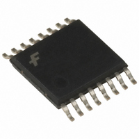
74VHC112MTC Fairchild Semiconductor, 74VHC112MTC Datasheet - Page 3

74VHC112MTC
Manufacturer Part Number
74VHC112MTC
Description
IC FLIP FLOP DUAL JK 16TSSOP
Manufacturer
Fairchild Semiconductor
Series
74VHCr
Type
JK Typer
Datasheet
1.74VHC112MTCX.pdf
(9 pages)
Specifications of 74VHC112MTC
Function
Set(Preset) and Reset
Output Type
Differential
Number Of Elements
2
Number Of Bits Per Element
1
Frequency - Clock
200MHz
Delay Time - Propagation
5.1ns
Trigger Type
Negative Edge
Current - Output High, Low
8mA, 8mA
Voltage - Supply
2 V ~ 5.5 V
Operating Temperature
-40°C ~ 85°C
Mounting Type
Surface Mount
Package / Case
16-TSSOP
Number Of Circuits
2
Logic Family
74VHC
Logic Type
J-K Flip-Flop
Polarity
Inverting/Non-Inverting
Input Type
Single-Ended
Propagation Delay Time
15 ns
High Level Output Current
- 8 mA
Supply Voltage (max)
5.5 V
Maximum Operating Temperature
+ 85 C
Mounting Style
SMD/SMT
Minimum Operating Temperature
- 40 C
Supply Voltage (min)
2 V
Lead Free Status / RoHS Status
Lead free / RoHS Compliant
Available stocks
Company
Part Number
Manufacturer
Quantity
Price
Company:
Part Number:
74VHC112MTCX
Manufacturer:
FAIRCHILD
Quantity:
548
Part Number:
74VHC112MTCX
Manufacturer:
FAIRCHILD/仙童
Quantity:
20 000
©1995 Fairchild Semiconductor Corporation
74VHC112 Rev. 1.2
Absolute Maximum Ratings
Stresses exceeding the absolute maximum ratings may damage the device. The device may not function or be
operable above the recommended operating conditions and stressing the parts to these levels is not recommended.
In addition, extended exposure to stresses above the recommended operating conditions may affect device reliability.
The absolute maximum ratings are stress ratings only.
Recommended Operating Conditions
The Recommended Operating Conditions table defines the conditions for actual device operation. Recommended
operating conditions are specified to ensure optimal performance to the datasheet specifications. Fairchild does not
recommend exceeding them or designing to absolute maximum ratings.
Note:
1. Unused inputs must be held HIGH or LOW. They may not float.
Symbol
Symbol
V
T
V
T
I
V
V
t
V
V
I
OUT
I
OUT
OPR
r
OUT
I
STG
T
OK
CC
CC
, t
CC
IK
IN
IN
L
f
Supply Voltage
Input Voltage
Output Voltage
Operating Temperature
Input Rise and Fall Time,
Supply Voltage
DC Input Voltage
DC Output Voltage
Input Diode Current
Output Diode Current
DC Output Current
DC V
Storage Temperature
Lead Temperature (Soldering, 10 seconds)
V
V
CC
CC
CC
= 3.3V ± 0.3V
= 5.0V ± 0.5V
/ GND Current
Parameter
Parameter
(1)
3
–0.5V to V
Rating
Rating
–65°C to +150°C
0ns/V ∼ 100ns/V
–40°C to +85°C
0ns/V ∼ 20ns/V
–0.5V to +7.0V
–0.5V to +7.0V
2.0V to +5.5V
www.fairchildsemi.com
0V to +5.5V
0V to V
CC
–20mA
±20mA
±25mA
±50mA
+ 0.5V
260°C
CC


