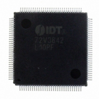
IDT72V3642L10PF IDT, Integrated Device Technology Inc, IDT72V3642L10PF Datasheet - Page 8

IDT72V3642L10PF
Manufacturer Part Number
IDT72V3642L10PF
Description
IC FIFO SYNC 3.3V CMOS 120-TQFP
Manufacturer
IDT, Integrated Device Technology Inc
Series
72Vr
Datasheet
1.IDT72V3642L10PF.pdf
(29 pages)
Specifications of IDT72V3642L10PF
Function
Synchronous
Memory Size
72M (1M x 72)
Data Rate
100MHz
Access Time
10ns
Voltage - Supply
3 V ~ 3.6 V
Operating Temperature
0°C ~ 70°C
Mounting Type
Surface Mount
Package / Case
120-TQFP, 120-VQFP
Lead Free Status / RoHS Status
Contains lead / RoHS non-compliant
Other names
72V3642L10PF
800-1534
800-1534
Available stocks
Company
Part Number
Manufacturer
Quantity
Price
Company:
Part Number:
IDT72V3642L10PF
Manufacturer:
IDT, Integrated Device Technology Inc
Quantity:
10 000
Company:
Part Number:
IDT72V3642L10PF8
Manufacturer:
IDT, Integrated Device Technology Inc
Quantity:
10 000
Commercial: V
TIMING REQUIREMENTS OVER RECOMMENDED RANGES OF SUPPLY
VOLTAGE AND OPERATING FREE-AIR TEMPERATURE
NOTES:
1. For 10ns speed grade only: V
2. Requirement to count the clock edge as one of at least four needed to reset a FIFO.
3. Skew time is not a timing constraint for proper device operation and is only included to illustrate the timing relationship between CLKA cycle and CLKB cycle.
4. Design simulated, not tested.
5. Industrial temperature range is available by special order.
IDT72V3622/72V3632/72V3642 CMOS 3.3V SyncBiFIFO
256 x 36 x 2, 512 x 36 x 2, 1,024 x 36 x 2
Symbol
f
t
t
t
t
t
t
t
t
t
t
t
t
t
t
t
S
DH
CLK
CLKH
CLKL
DS
ENS1
ENS2
FSS
FWS
ENH
RSTH
FSH
SKEW1
SKEW2
RSTS
(3,4)
(3)
Clock Frequency, CLKA or CLKB
Clock Cycle Time, CLKA or CLKB
Pulse Duration, CLKA or CLKB HIGH
Pulse Duration, CLKA and CLKB LOW
Setup Time, A0-A35 before CLKA↑ and B0-B35 before CLKB↑
Setup Time CSA before CLKA↑; CSB before CLKB↑
Setup Time ENA, W/RA and MBA before CLKA↑; ENB, W/RB and MBB
before CLKB↑
Setup Time, RST1 or RST2 LOW before CLKA↑ or CLKB↑
Setup Time, FS0 and FS1 before RST1 and RST2 HIGH
Setup Time, FWFT before CLKA↑
Hold Time, A0-A35 after CLKA↑ and B0-B35 after CLKB↑
Hold Time, CSA, W/RA, ENA, and MBA after CLKA↑; CSB, W/RB, ENB, and
MBB after CLKB↑
Hold Time, RST1 or RST2 LOW after CLKA↑ or CLKB↑
Hold Time, FS0 and FS1 after RST1 and RST2 HIGH
Skew Time, between CLKA↑ and CLKB↑ for EFA/ORA, EFB/ORB, FFA/IRA,
and FFB/IRB
Skew Time, between CLKA↑ and CLKB↑ for AEA, AEB, AFA, and AFB
CC
=3.3V± 0.30V; for 10ns (100 MHz) operation, V
CC
= 3.3V +/- 0.15V, T
Parameter
A
= 0° ° ° ° ° to +70° ° ° ° ° C; JEDEC JESD8-A compliant.
CC
TM
=3.3V ±0.15V; T
(2)
(2)
8
A
= 0
ο
C to +70
ο
C; JEDEC JESD8-A compliant
IDT72V3622L10
IDT72V3632L10
IDT72V3642L10
Min.
4.5
4.5
7.5
0.5
0.5
7.5
—
10
12
3
4
3
5
0
4
2
COMMERCIAL TEMPERATURE RANGE
Max.
100
—
—
—
—
—
—
—
—
—
—
—
—
—
—
—
(1)
(1)
(1)
IDT72V3622L15
IDT72V3632L15
IDT72V3642L15
Min.
4.5
4.5
7.5
7.5
15
12
—
6
6
4
5
0
1
1
4
2
Max.
66.7
—
—
—
—
—
—
—
—
—
—
—
—
—
—
—
Unit
MHz
ns
ns
ns
ns
ns
ns
ns
ns
ns
ns
ns
ns
ns
ns
ns


