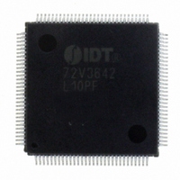
IDT72V3642L10PF IDT, Integrated Device Technology Inc, IDT72V3642L10PF Datasheet - Page 6

IDT72V3642L10PF
Manufacturer Part Number
IDT72V3642L10PF
Description
IC FIFO SYNC 3.3V CMOS 120-TQFP
Manufacturer
IDT, Integrated Device Technology Inc
Series
72Vr
Datasheet
1.IDT72V3642L10PF.pdf
(29 pages)
Specifications of IDT72V3642L10PF
Function
Synchronous
Memory Size
72M (1M x 72)
Data Rate
100MHz
Access Time
10ns
Voltage - Supply
3 V ~ 3.6 V
Operating Temperature
0°C ~ 70°C
Mounting Type
Surface Mount
Package / Case
120-TQFP, 120-VQFP
Lead Free Status / RoHS Status
Contains lead / RoHS non-compliant
Other names
72V3642L10PF
800-1534
800-1534
Available stocks
Company
Part Number
Manufacturer
Quantity
Price
Company:
Part Number:
IDT72V3642L10PF
Manufacturer:
IDT, Integrated Device Technology Inc
Quantity:
10 000
Company:
Part Number:
IDT72V3642L10PF8
Manufacturer:
IDT, Integrated Device Technology Inc
Quantity:
10 000
ABSOLUTE MAXIMUM RATINGS OVER OPERATING FREE-AIR
TEMPERATURE RANGE (Unless otherwise noted)
NOTES:
1. Stresses beyond those listed under "Absolute Maximum Ratings" may cause permanent damage to the device. These are stress ratings only and functional operation of the device at these
2. The input and output voltage ratings may be exceeded provided the input and output current ratings are observed.
NOTE:
ELECTRICAL CHARACTERISTICS OVER RECOMMENDED OPERATING
FREE-AIR TEMPERATURE RANGE (Unless otherwise noted)
RECOMMENDED OPERATING CONDITIONS
1. For 10ns (100 MHz operation), Vcc=3.3V +/- 0.15V, T
NOTES:
1. For 10ns speed grade only: V
2. All typical values are at V
3. For additional I
4. Characterized values, not currently tested.
5. Industrial temperature range is available by special order.
IDT72V3622/72V3632/72V3642 CMOS 3.3V SyncBiFIFO
256 x 36 x 2, 512 x 36 x 2, 1,024 x 36 x 2
Symbol
V
or any other conditions beyond those indicated under "recommended operating conditions" is not implied. Exposure to absolute maximum rated conditions for extended periods may affect
device reliability.
V
V
I
I
Symbol
CC
Symbol
T
OH
OL
IH
IL
A
V
V
V
I
I
I
T
V
V
I
I
I
I
C
C
CC
LI
CC2
CC3
I
OK
OUT
LO
(1)
IK
STG
CC
I
O
OH
OL
IN
OUT
(2)
(2)
(4)
(3)
(3)
(4)
Supply Voltage
High-Level Input Voltage
Low-Level Input Voltage
High-Level Output Current
Low-Level Output Current
Operating Temperature
Output Logic "1" Voltage
Output Logic "0" Voltage
Input Leakage Current (Any Input)
Output Leakage Current
Standby Current (with CLKA and CLKB running)
Standby Current (no clocks running)
Input Capacitance
Output Capacitance
CC
Supply Voltage Range
Input Voltage Range
Output Voltage Range
Input Clamp Current (V
Output Clamp Current (V
Continuous Output Current (V
Continuous Current Through V
Storage Temperature Range
information, see Figure 1, Typical Characteristics: Supply Current (I
Parameter
CC
= 3.3V, T
CC
= 3.3V +/- 0.15V, T
Parameter
A
I
= 25° ° ° ° ° C.
< 0 or V
O
= < 0 or V
O
CC
Min.
= 0 to V
I
A
3.0
or GND
> V
—
—
—
= 0° to +70°C; JEDEC JESD8-A compliant.
2
0
A
CC
O
= 0° ° ° ° ° to +70° ° ° ° ° C; JEDEC JESD8-A compliant.
CC
> V
)
)
Typ.
CC
3.3
—
—
—
—
—
)
Rating
V
V
V
V
V
V
V
V
V
Max.
TM
CC
CC
CC
CC
CC
CC
CC
I
O
3.6
0.8
–4
70
= 0,
8
+0.5
= 0,
= 3.0V,
= 3.0V,
= 3.6V,
= 3.6V,
= 3.6V,
= 3.6V,
Unit
mA
mA
6
°
V
V
V
C
Test Conditions
CC
) vs. Clock Frequency (f
I
I
V
V
V
V
f = 1 MHz
f = 1 MHZ
OH
OL
I
O
I
I
= V
= V
= V
= V
= 8 mA
= –4 mA
CC
CC
CC
CC
or 0
- 0.2V or 0
- 0.2V or 0
or 0
(1)
S
).
COMMERCIAL TEMPERATURE RANGE
Min.
2.4
—
—
—
—
—
—
—
t
CLK
–0.5 to V
–0.5 to V
Commercial
IDT72V3622
IDT72V3632
IDT72V3642
Commercial
–0.5 to +4.6
–65 to 150
= 10
Typ.
±400
±20
±50
±50
—
—
—
—
—
—
4
8
CC
CC
(1)
(2)
, 15ns
+0.5
+0.5
Max.
±10
±10
0.5
—
—
—
5
1
Unit
mA
mA
mA
ο ο ο ο ο
mA
Unit
V
V
V
µ A
µ A
mA
mA
C
pF
pF
V
V


