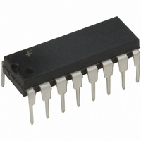
CD4060BCN Fairchild Semiconductor, CD4060BCN Datasheet - Page 4

CD4060BCN
Manufacturer Part Number
CD4060BCN
Description
IC COUNTER BIN RIP 14ST 16-DIP
Manufacturer
Fairchild Semiconductor
Series
4000Br
Datasheet
1.CD4060BCMX.pdf
(8 pages)
Specifications of CD4060BCN
Logic Type
Binary Counter
Direction
Up
Number Of Elements
1
Number Of Bits Per Element
14
Reset
Asynchronous
Count Rate
12MHz
Trigger Type
Negative Edge
Voltage - Supply
3 V ~ 15 V
Operating Temperature
-55°C ~ 125°C
Mounting Type
Through Hole
Package / Case
16-DIP (0.300", 7.62mm)
Counter Type
Binary Counters
Logic Family
4060
Operating Temperature Range
- 55 C to + 125 C
Mounting Style
Through Hole
Lead Free Status / RoHS Status
Lead free / RoHS Compliant
Timing
-
Lead Free Status / Rohs Status
Lead free / RoHS Compliant
Other names
4060
4060B
4060B
Available stocks
Company
Part Number
Manufacturer
Quantity
Price
Company:
Part Number:
CD4060BCN
Manufacturer:
TI
Quantity:
3 400
Part Number:
CD4060BCN
Manufacturer:
NS/国半
Quantity:
20 000
www.fairchildsemi.com
I
V
V
V
V
I
I
I
DD
OL
OH
IN
Symbol
Absolute Maximum Ratings
(Note 2)
DC Electrical Characteristics
Note 3: Data does not apply to oscillator points
OL
OH
IL
IH
Supply Voltage (V
Input Voltage (V
Storage Temperature Range (T
Package Dissipation (P
Lead Temperature (T
Dual-In-Line
Small Outline
(Soldering, 10 seconds)
Quiescent Device Current
LOW Level Output Voltage
HIGH Level Output Voltage
LOW Level Input Voltage
HIGH Level Input Voltage
LOW Level Output Current
(Note 3)
HIGH Level Output Current
(Note 3)
Input Current
IN
Parameter
)
DD
)
L
)
D
)
S
)
V
V
V
V
V
V
V
V
V
V
V
V
V
V
V
V
V
V
V
V
V
V
V
0
DD
DD
DD
DD
DD
DD
DD
DD
DD
DD
DD
DD
DD
DD
DD
DD
DD
DD
DD
DD
DD
DD
DD
and
0.5V to V
5V, V
10V, V
15V, V
5V
10V
15V
5V
10V
15V
5V, V
10V, V
15V, V
5V, V
10V, V
15V, V
5V, V
10V, V
15V, V
5V, V
10V, V
15V, V
15V, V
15V, V
65 C to 150 C
0
of CD4060BC. I
(Note 1)
0.5V to 18V
Conditions
IN
O
O
O
O
IN
IN
O
O
O
O
O
O
O
O
IN
IN
(Note 2)
DD
700 mW
500 mW
0.5V or 4.5V
0.5V or 4.5V
0.4V
4.6V
V
1.0V or 9.0V
1.5V or 13.5V
1.0V or 9.0V
1.5V or 13.5V
0.5V
1.5V
9.5V
13.5V
V
V
0V
15V
DD
260 C
DD
DD
0.5V
or V
or V
or V
OH
SS
and I
SS
SS
4
Recommended Operating
Conditions
Note 1: “Absolute Maximum Ratings” are those values beyond which the
safety of the device cannot be guaranteed. They are not meant to imply
that the devices should be operated at these limits. The tables of “Recom-
mended Operating Conditions” and “Electrical Characteristics” provide con-
ditions for actual device operation.
Note 2: V
Supply Voltage (V
Input Voltage (V
Operating Temperature Range (T
OL
are tested one output at a time.
14.95
4.95
9.95
11.0
0.52
Min
3.5
7.0
1.3
3.6
0.52
1.3
3.6
SS
40 C
0V unless otherwise specified.
0.05
0.05
0.05
0.30
Max
1.5
3.0
4.0
0.30
20
40
80
IN
)
DD
14.95
4.95
9.95
11.0
0.44
Min
3.5
7.0
1.1
3.0
0.44
1.1
3.0
)
0.88
2.25
10
25 C
Typ
10
8.8
0.88
2.25
10
15
8.8
0
0
0
5
2
4
6
3
6
9
5
5
A
Max
0.05
0.05
0.05
0.30
1.5
3.0
4.0
0.30
)
20
40
80
14.95
4.95
9.95
11.0
0.36
Min
3.5
7.0
0.9
2.4
0.36
0.9
2.4
40 C to 85 C
85 C
3V to 15V
Max
0.05
0.05
0.05
0V to V
150
300
600
1.5
3.0
4.0
1.0
1.0
Units
DD
mA
mA
mA
mA
mA
mA
V
V
V
V
V
V
V
V
V
V
V
V
A
A
A
A
A


