MM74C85N Fairchild Semiconductor, MM74C85N Datasheet - Page 3
MM74C85N
Manufacturer Part Number
MM74C85N
Description
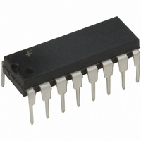
IC COMPARATOR MAGNITUDE 4B 16DIP
Manufacturer
Fairchild Semiconductor
Series
74Cr
Type
Magnitude Comparatorr
Datasheet
1.MM74C85N.pdf
(5 pages)
Specifications of MM74C85N
Number Of Bits
4
Delay Time - Propagation
100ns
Current - Supply
300µA
Voltage - Supply
3 V ~ 15 V
Operating Temperature
-55°C ~ 125°C
Package / Case
16-DIP (0.300", 7.62mm)
Lead Free Status / RoHS Status
Lead free / RoHS Compliant
Other names
74C85
74C85N
74C85N
Available stocks
Company
Part Number
Manufacturer
Quantity
Price

Part Number:
MM74C85N
Manufacturer:
NS/国半
Quantity:
20 000


CMOS TO CMOS
V
V
V
V
I
I
I
CMOS/LPTTL INTERFACE
V
V
V
V
OUTPUT DRIVE (See Family Characteristics Data Sheet) (Short Circuit Current)
I
I
I
I
t
t
C
C
IN(1)
IN(0)
CC
SOURCE
SOURCE
SINK
SINK
pd
pd
Absolute Maximum Ratings
DC Electrical Characteristics
Min/Max limits apply across temperature range unless otherwise noted
AC Electrical Characteristics
T
Note 2: AC Parameters are guaranteed by DC correlated testing.
Note 3: Capacitance is guaranteed by periodic testing.
Note 4: C
AN-90.
IN(1)
IN(0)
OUT(1)
OUT(0)
IN(1)
IN(0)
OUT(1)
OUT(0)
IN
PD
Voltage at Any Pin
Operating Temperature Range
Storage Temperature Range
Power Dissipation (P
Operating V
Symbol
Symbol
A
Dual-In-Line
Small Outline
25 C, C
PD
determines the no load AC power consumption of any CMOS device. For complete explanation see Family Characteristics application note,
Logical “1” Input Voltage
Logical “0” Input Voltage
Logical “1” Output Voltage
Logical “0” Output Voltage
Logical “1” Input Current
Logical “0” Input Current
Supply Current
Logical “1” Input Voltage
Logical “0” Input Voltage
Logical “1” Output Voltage
Logical “0” Output Voltage
Output Source Current
(P-Channel)
Output Source Current
(P-Channel)
Output Sink Current
(N-Channel)
Output Sink Current
(N-Channel)
Propagation Delay from any A
or B Data Input to any Data Output
Propagation Delay Time from
any Cascade Input to any Output
Input Capacitance
Power Dissipation Capacitance
CC
L
50 pF, unless otherwise specified
Range
D
Parameter
Parameter
)
0.3V to V
55 C to 125 C
65 C to 150 C
V
V
V
V
V
V
V
V
V
V
V
V
V
V
V
V
T
V
T
V
T
V
T
V
V
V
V
Any Input
Per Package (Note 4)
(Note 1)
A
A
A
A
CC
CC
CC
CC
CC
CC
CC
CC
CC
CC
CC
CC
CC
CC
CC
CC
CC
CC
CC
CC
CC
CC
CC
3.0V to 15V
25 C
25 C
25 C
25 C
CC
(Note 2)
5.0V
10V
5.0V
10V
5.0V, I
10V, I
5.0V, I
10V, I
15V, V
15V, V
15V
4.75V
4.75V
4.75V, I
4.75V, I
5.0V, V
10V, V
5.0V, V
10V, V
50V
10V
50V
10V
700 mW
500 mW
0.3V
O
O
O
O
IN
IN
OUT
OUT
OUT
OUT
Conditions
Conditions
O
O
10 A
10 A
15V
0V
10 A
10 A
360 A
3
360 A
0V
V
0V
V
Note 1: “Absolute Maximum Ratings” are those values beyond which the
safety of the device cannot be guaranteed. Except for “Operating Tempera-
ture Range” they are not meant to imply that the devices should be oper-
ated at these limits. The table of “Electrical Characteristics” provides
conditions for actual device operation.
CC
V
Lead Temperature
CC
CC
(Soldering, 10 seconds)
V
CC
1.75
Min
Min
3.5
8.0
4.5
9.0
2.4
1.75
8.0
1.0
8.0
1.5
0.005
0.005
0.05
Typ
Typ
250
100
200
100
3.6
5.0
16
45
3.3
15
www.fairchildsemi.com
Max
Max
300
600
300
500
250
1.5
2.0
0.5
1.0
1.0
0.8
0.4
260 C
Units
Units
mA
mA
mA
mA
pF
pF
ns
ns
18V
V
V
V
V
V
V
V
V
A
A
A
Related parts for MM74C85N
Image
Part Number
Description
Manufacturer
Datasheet
Request
R

Part Number:
Description:
Fairchild Semiconductor [IGBT MODULE]
Manufacturer:
Fairchild Semiconductor
Datasheet:

Part Number:
Description:
Discrete Semiconductor Modules
Manufacturer:
Fairchild Semiconductor
Part Number:
Description:
Discrete Semiconductor Modules
Manufacturer:
Fairchild Semiconductor
Part Number:
Description:
This N-Channel MOSFET is produced using Fairchild Semiconductor’s advanced Power Trench® process
Manufacturer:
Fairchild Semiconductor
Datasheet:
Part Number:
Description:
This N-Channel MOSFET is produced using Fairchild Semiconductor’s advanced Power Trench® process
Manufacturer:
Fairchild Semiconductor
Datasheet:
Part Number:
Description:
This N-Channel MOSFET is produced using Fairchild Semiconductor’s advanced PowerTrench® process
Manufacturer:
Fairchild Semiconductor
Datasheet:
Part Number:
Description:
This N-Channel MOSFET is produced using Fairchild Semiconductor’s advanced PowerTrench® process
Manufacturer:
Fairchild Semiconductor
Datasheet:
Part Number:
Description:
This N-Channel MOSFET is produced using Fairchild Semiconductor’s advanced Power Trench® process
Manufacturer:
Fairchild Semiconductor
Datasheet:
Part Number:
Description:
This N-Channel logic Level MOSFETs are produced using Fairchild Semiconductor‘s advanced Power Trench® process that has been special tailored to minimize the on-state resistance and yet maintain superior switching performance
Manufacturer:
Fairchild Semiconductor
Datasheet:
Part Number:
Description:
This N-Channel MOSFET is produced using Fairchild Semiconductor’s advanced Power Trench® process
Manufacturer:
Fairchild Semiconductor
Datasheet:
Part Number:
Description:
This N-Channel SyncFET™ is produced using Fairchild Semiconductor’s advanced PowerTrench® process
Manufacturer:
Fairchild Semiconductor
Datasheet:
Part Number:
Description:
This N-Channel SyncFET™ is produced using Fairchild Semiconductor’s advanced PowerTrench® process
Manufacturer:
Fairchild Semiconductor
Datasheet:
Part Number:
Description:
This N-Channel SyncFET™ is produced using Fairchild Semiconductor’s advanced PowerTrench® process
Manufacturer:
Fairchild Semiconductor
Datasheet:
Part Number:
Description:
This N-Channel logic Level MOSFETs are produced using Fairchild Semiconductor‘s advanced Power Trench® process that has been special tailored to minimize the on-state resistance and yet maintain superior switching performance
Manufacturer:
Fairchild Semiconductor
Datasheet:
Part Number:
Description:
This N-Channel MOSFET is produced using Fairchild Semiconductor’s advanced Power Trench® process that has been especially tailored to minimize the on-state resistance and yet maintain superior switching performance
Manufacturer:
Fairchild Semiconductor
Datasheet: