74VCX164245MTDX Fairchild Semiconductor, 74VCX164245MTDX Datasheet - Page 2
74VCX164245MTDX
Manufacturer Part Number
74VCX164245MTDX
Description
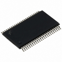
IC TRANSCEIVER 16BIT 48TSSOP
Manufacturer
Fairchild Semiconductor
Series
74VCXr
Datasheet
1.74VCX164245MTDX.pdf
(9 pages)
Specifications of 74VCX164245MTDX
Logic Type
Transceiver, Non-Inverting
Number Of Elements
2
Number Of Bits Per Element
8
Operating Temperature
-40°C ~ 85°C
Mounting Type
Surface Mount
Package / Case
48-TSSOP
Number Of Circuits
1
Logic Family
74VC
Polarity
Non-Inverting
Output Type
3-State
Propagation Delay Time
6.2 ns
High Level Output Current
- 24 mA
Low Level Output Current
24 mA
Supply Voltage (max)
2.7 V, 3.6 V
Maximum Operating Temperature
+ 85 C
Mounting Style
SMD/SMT
Minimum Operating Temperature
- 40 C
Supply Voltage (min)
1.65 V, 2.3 V
Lead Free Status / RoHS Status
Lead free / RoHS Compliant
Voltage - Supply
-
Current - Output High, Low
-
Lead Free Status / Rohs Status
Lead free / RoHS Compliant


www.fairchildsemi.com
Connection Diagrams
Translator Power Up Sequence Recommendations
To guard against power up problems, some simple guide-
lines need to be adhered to. The VCX164245 is designed
so that the control pins (T/R
Therefore the first recommendation is to begin by powering
up the control side of the device, V
pins should be ramped with or ahead of V
guard against bus contentions and oscillations as all A Port
and B Port outputs will be disabled. To ensure the high
impedance state during power up or power down, OE
should be tied to V
mum value of the resistor is determined by the current
Pin Assignment for TSSOP
Pin Assignment for FBGA
CCB
(Top Through View)
through a pull up resistor. The mini-
n
, OE
n
) are supplied by V
CCB
. The OE
CCB
, this will
n
control
CCB
n
.
2
Pin Descriptions
FBGA Pin Assignments
Truth Tables
H
L
X
Z
sourcing capability of the driver. Second, the T/R
pins should be placed at logic low (0V) level, this will
ensure that the B-side bus pins are configured as inputs to
help guard against bus contention and oscillations. B-side
Data Inputs should be driven to a valid logic level (0V or
V
tions. V
never exceed the V
these steps the device can then be configured for the users
desired operation. Following these steps will help to pre-
vent possible damage to the translator device as well as
other system components.
Pin Names
OE
T/R
A
B
NC
CCB
0
0
LOW Voltage Level
High Impedance
HIGH Voltage Level
Immaterial (HIGH or LOW, inputs may not float)
–A
–B
OE
OE
G
A
B
C
D
E
F
H
n
J
n
H
H
L
L
L
L
), this will prevent excessive current draw and oscilla-
15
15
1
2
CCA
Inputs
Inputs
B
B
B
B
B
B
B
B
B
can then be powered up after V
1
10
12
14
15
0
2
4
6
8
T/R
T/R
H
H
L
X
L
X
Output Enable Input (Active LOW)
Transmit/Receive Input
Side A Inputs or 3-STATE Outputs
Side B Inputs or 3-STATE Outputs
No Connect
1
2
NC
B
B
NC
CCB
B
B
B
B
B
2
11
13
1
3
5
7
9
Bus B
Bus A
HIGH Z State on A
Bus B
Bus A
HIGH-Z State on A
voltage level. Upon completion of
V
V
GND
GND
GND
T/R
T/R
NC
NC
0
0
8
8
CCB
CCB
3
–B
–A
–B
–A
1
2
Description
7
7
15
15
Data to Bus A
Data to Bus B
Data to Bus A
Data to Bus B
V
V
GND
GND
GND
OE
OE
Outputs
Outputs
NC
NC
CCA
CCA
4
1
2
0
8
–A
–A
CCB
7
15
A
NC
A
NC
A
A
A
A
A
, B
5
, but should
11
13
, B
1
3
5
7
9
0
0
–A
–B
0
8
8
–B
–A
–B
8
n
–B
7
7
control
7
15
15
A
A
A
A
15
A
A
A
A
A
6
10
12
14
15
0
2
4
6
8
Related parts for 74VCX164245MTDX
Image
Part Number
Description
Manufacturer
Datasheet
Request
R

Part Number:
Description:
Fairchild Semiconductor [IGBT MODULE]
Manufacturer:
Fairchild Semiconductor
Datasheet:

Part Number:
Description:
Discrete Semiconductor Modules
Manufacturer:
Fairchild Semiconductor
Part Number:
Description:
Discrete Semiconductor Modules
Manufacturer:
Fairchild Semiconductor
Part Number:
Description:
This N-Channel MOSFET is produced using Fairchild Semiconductor’s advanced Power Trench® process
Manufacturer:
Fairchild Semiconductor
Datasheet:
Part Number:
Description:
This N-Channel MOSFET is produced using Fairchild Semiconductor’s advanced Power Trench® process
Manufacturer:
Fairchild Semiconductor
Datasheet:
Part Number:
Description:
This N-Channel MOSFET is produced using Fairchild Semiconductor’s advanced PowerTrench® process
Manufacturer:
Fairchild Semiconductor
Datasheet:
Part Number:
Description:
This N-Channel MOSFET is produced using Fairchild Semiconductor’s advanced PowerTrench® process
Manufacturer:
Fairchild Semiconductor
Datasheet:
Part Number:
Description:
This N-Channel MOSFET is produced using Fairchild Semiconductor’s advanced Power Trench® process
Manufacturer:
Fairchild Semiconductor
Datasheet:
Part Number:
Description:
This N-Channel logic Level MOSFETs are produced using Fairchild Semiconductor‘s advanced Power Trench® process that has been special tailored to minimize the on-state resistance and yet maintain superior switching performance
Manufacturer:
Fairchild Semiconductor
Datasheet:
Part Number:
Description:
This N-Channel MOSFET is produced using Fairchild Semiconductor’s advanced Power Trench® process
Manufacturer:
Fairchild Semiconductor
Datasheet:
Part Number:
Description:
This N-Channel SyncFET™ is produced using Fairchild Semiconductor’s advanced PowerTrench® process
Manufacturer:
Fairchild Semiconductor
Datasheet:
Part Number:
Description:
This N-Channel SyncFET™ is produced using Fairchild Semiconductor’s advanced PowerTrench® process
Manufacturer:
Fairchild Semiconductor
Datasheet:
Part Number:
Description:
This N-Channel SyncFET™ is produced using Fairchild Semiconductor’s advanced PowerTrench® process
Manufacturer:
Fairchild Semiconductor
Datasheet:
Part Number:
Description:
This N-Channel logic Level MOSFETs are produced using Fairchild Semiconductor‘s advanced Power Trench® process that has been special tailored to minimize the on-state resistance and yet maintain superior switching performance
Manufacturer:
Fairchild Semiconductor
Datasheet:
Part Number:
Description:
This N-Channel MOSFET is produced using Fairchild Semiconductor’s advanced Power Trench® process that has been especially tailored to minimize the on-state resistance and yet maintain superior switching performance
Manufacturer:
Fairchild Semiconductor
Datasheet: