MM74C906M Fairchild Semiconductor, MM74C906M Datasheet - Page 3
MM74C906M
Manufacturer Part Number
MM74C906M
Description
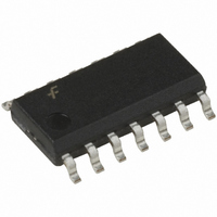
IC BUFFER HEX OP/DR N-INV 14SOIC
Manufacturer
Fairchild Semiconductor
Series
74Cr
Specifications of MM74C906M
Logic Type
Buffer/Line Driver, Non-Inverting with Open Drain
Number Of Elements
6
Number Of Bits Per Element
1
Voltage - Supply
3 V ~ 15 V
Operating Temperature
-40°C ~ 85°C
Mounting Type
Surface Mount
Package / Case
14-SOIC (3.9mm Width), 14-SOL
Logic Family
74C
Number Of Channels Per Chip
Hex
Polarity
Non-Inverting
Supply Voltage (max)
15 V
Supply Voltage (min)
3 V
Maximum Operating Temperature
85 C
Mounting Style
SMD/SMT
Maximum Power Dissipation
500 mW
Minimum Operating Temperature
- 40 C
Output Type
Open Drain
Propagation Delay Time
150 ns @ 5 V or 75 ns @ 10 V
Number Of Lines (input / Output)
6 / 6
Lead Free Status / RoHS Status
Lead free / RoHS Compliant
Current - Output High, Low
-
Lead Free Status / Rohs Status
Lead free / RoHS Compliant
Available stocks
Company
Part Number
Manufacturer
Quantity
Price
Company:

Part Number:
MM74C906M
Manufacturer:
Fairchild Semiconductor
Quantity:
668
Part Number:
MM74C906M
Manufacturer:
NS/国半
Quantity:
20 000
Part Number:
MM74C906MX
Manufacturer:
FAI
Quantity:
20 000


t
t
C
C
C
pd
pd
AC Electrical Characteristics
T
Note 2: AC Parameters are guaranteed by DC correlated testing.
Note 3: “C” used in calculating propagation includes output load capacity (C
Note 4: Capacitance is guaranteed by periodic testing.
Note 5: C
AN-90. (Assumes outputs are open).
Typical Applications
Note: Can be extended to more than 2 inputs.
Note: V
V
IN
OUT
PD
Symbol
A
CC
25 C, C
15V
CC
PD
Propagation Delay Time
to a Logical “0”
Propagation Delay Time
to a Logical “1”
Input Capacitance
Output Capacity
Power Dissipation Capacity
V
determines the no load AC power consumption of any CMOS device. For complete explanation see Family Characteristics Application Note,
DD
MM74C906
MM74C907
MM74C906
MM74C907
CMOS or TTL to PMOS Interface
L
18V
50 pF, unless otherwise specified
Wire OR Gate
Parameter
V
V
V
V
(Note 5) Per Buffer
V
V
V
V
(Note 4)
(Note 4)
CC
CC
CC
CC
CC
CC
CC
CC
(Note 2)
10V, R
5.0V, R
5.0V (Note 3)
10V (Note 3)
5.0V (Note 3)
10V (Note 3)
5.0V, R
10V, R
Conditions
10k
10k
L
10k
10k
) plus device output capacity (C
3
Note: Can be extended to more than 2 inputs.
CMOS or TTL to CMOS at a Higher V
Min
Wire AND Gate
OUT
).
Typ
5.0
20
30
150
150
www.fairchildsemi.com
75
75
Max
150
150
75
75
0.7 RC
0.7 RC
0.7 RC
0.7 RC
CC
Units
pF
pF
pF
ns
ns
ns
ns
ns
ns
ns
ns
Related parts for MM74C906M
Image
Part Number
Description
Manufacturer
Datasheet
Request
R

Part Number:
Description:
Fairchild Semiconductor [IGBT MODULE]
Manufacturer:
Fairchild Semiconductor
Datasheet:

Part Number:
Description:
Discrete Semiconductor Modules
Manufacturer:
Fairchild Semiconductor
Part Number:
Description:
Discrete Semiconductor Modules
Manufacturer:
Fairchild Semiconductor
Part Number:
Description:
This N-Channel MOSFET is produced using Fairchild Semiconductor’s advanced Power Trench® process
Manufacturer:
Fairchild Semiconductor
Datasheet:
Part Number:
Description:
This N-Channel MOSFET is produced using Fairchild Semiconductor’s advanced Power Trench® process
Manufacturer:
Fairchild Semiconductor
Datasheet:
Part Number:
Description:
This N-Channel MOSFET is produced using Fairchild Semiconductor’s advanced PowerTrench® process
Manufacturer:
Fairchild Semiconductor
Datasheet:
Part Number:
Description:
This N-Channel MOSFET is produced using Fairchild Semiconductor’s advanced PowerTrench® process
Manufacturer:
Fairchild Semiconductor
Datasheet:
Part Number:
Description:
This N-Channel MOSFET is produced using Fairchild Semiconductor’s advanced Power Trench® process
Manufacturer:
Fairchild Semiconductor
Datasheet:
Part Number:
Description:
This N-Channel logic Level MOSFETs are produced using Fairchild Semiconductor‘s advanced Power Trench® process that has been special tailored to minimize the on-state resistance and yet maintain superior switching performance
Manufacturer:
Fairchild Semiconductor
Datasheet:
Part Number:
Description:
This N-Channel MOSFET is produced using Fairchild Semiconductor’s advanced Power Trench® process
Manufacturer:
Fairchild Semiconductor
Datasheet:
Part Number:
Description:
This N-Channel SyncFET™ is produced using Fairchild Semiconductor’s advanced PowerTrench® process
Manufacturer:
Fairchild Semiconductor
Datasheet:
Part Number:
Description:
This N-Channel SyncFET™ is produced using Fairchild Semiconductor’s advanced PowerTrench® process
Manufacturer:
Fairchild Semiconductor
Datasheet:
Part Number:
Description:
This N-Channel SyncFET™ is produced using Fairchild Semiconductor’s advanced PowerTrench® process
Manufacturer:
Fairchild Semiconductor
Datasheet:
Part Number:
Description:
This N-Channel logic Level MOSFETs are produced using Fairchild Semiconductor‘s advanced Power Trench® process that has been special tailored to minimize the on-state resistance and yet maintain superior switching performance
Manufacturer:
Fairchild Semiconductor
Datasheet:
Part Number:
Description:
This N-Channel MOSFET is produced using Fairchild Semiconductor’s advanced Power Trench® process that has been especially tailored to minimize the on-state resistance and yet maintain superior switching performance
Manufacturer:
Fairchild Semiconductor
Datasheet: