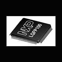
LPC2921_23_25 NXP Semiconductors, LPC2921_23_25 Datasheet - Page 8

LPC2921_23_25
Manufacturer Part Number
LPC2921_23_25
Description
The LPC2921/2923/2925 combine an ARM968E-S CPU core with two integrated TCMblocks operating at frequencies of up to 125 MHz, Full-speed USB 2
Manufacturer
NXP Semiconductors
Datasheet
1.LPC2921_23_25.pdf
(84 pages)
- Current page: 8 of 84
- Download datasheet (552Kb)
NXP Semiconductors
Table 3.
LPC2921_23_25_3
Product data sheet
Pin name
V
JTAGSEL
n.c.
VREFP
VREFN
P0[8]/IN1[0]
P0[9]/IN1[1]
P0[10]/IN1[2]/
PMAT1[0]
P0[11]/IN1[3]/
PMAT1[1]
V
P0[12]/IN1[4]/
PMAT1[2]
P0[13]/IN1[5]/
PMAT1[3]
P0[14]/IN1[6]/
PMAT1[4]
P0[15]/IN1[7]/
PMAT1[5]
P0[16]IN2[0]/TXD0
P0[17]/IN2[1]/
RXD0/A23
V
V
V
P0[18]/IN2[2]/
PMAT2[0]
P0[19]/IN2[3]/
PMAT2[1]
P0[20]/IN2[4]/
PMAT2[2]
P0[21]/IN2[5]/
PMAT2[3]
P0[22]/IN2[6]/
PMAT2[4]/A18
V
DDA(ADC3V3)
SS(IO)
DD(CORE)
SS(CORE)
DD(IO)
SS(IO)
LQFP100 pin assignment
Pin
74
75
76
77
78
79
80
81
82
83
84
85
86
87
88
89
90
91
92
93
94
95
96
97
98
[1]
[3]
[3]
[4]
[4]
[4]
[4]
[4]
[4]
[4]
[4]
[4]
[4]
[4]
[4]
[4]
[4]
[4]
Description
Function 0 (default)
3.3 V power supply for ADC
TAP controller select input; LOW-level selects the ARM debug mode; HIGH-level selects
boundary scan; pulled up internally.
not connected to a function; must be tied to 3.3 V power supply for ADC V
HIGH reference for ADC
LOW reference for ADC
GPIO0, pin 8
GPIO0, pin 9
GPIO0, pin 10
GPIO0, pin 11
ground for I/O
GPIO0, pin 12
GPIO0, pin 13
GPIO0, pin 14
GPIO0, pin 15
GPIO0, pin 16
GPIO0, pin 17
1.8 V power supply for digital core
ground for digital core
3.3 V power supply for I/O
GPIO0, pin 18
GPIO0, pin 19
GPIO0, pin 20
GPIO0, pin 21
GPIO0, pin 22
ground for I/O
…continued
All information provided in this document is subject to legal disclaimers.
Rev. 03 — 14 April 2010
Function 1
ADC1 IN0
ADC1 IN1
ADC1 IN2
ADC1 IN3
ADC1 IN4
ADC1 IN5
ADC1 IN6
ADC1 IN7
ADC2 IN0
ADC2 IN1
ADC2 IN2
ADC2 IN3
ADC2 IN4
ADC2 IN5
ADC2 IN6
ARM9 microcontroller with CAN, LIN, and USB
LPC2921/2923/2925
Function 2
-
-
PWM1 MAT0
PWM1 MAT1
PWM1 MAT2
PWM1 MAT3
PWM1 MAT4
PWM1 MAT5
UART0 TXD
UART0 RXD
PWM2 MAT0
PWM2 MAT1
PWM2 MAT2
PWM2 MAT3
PWM2 MAT4
© NXP B.V. 2010. All rights reserved.
Function 3
-
-
-
-
-
-
-
-
-
-
-
-
-
-
-
DDA(ADC3V3)
8 of 84
.
Related parts for LPC2921_23_25
Image
Part Number
Description
Manufacturer
Datasheet
Request
R
Part Number:
Description:
Arm9 Microcontroller With Can, Lin, And Usb Device
Manufacturer:
NXP Semiconductors
Datasheet:
Part Number:
Description:
(LPC2921 - LPC2925) ARM9 microcontroller
Manufacturer:
NXP Semiconductors
Datasheet:
Part Number:
Description:
NXP Semiconductors designed the LPC2420/2460 microcontroller around a 16-bit/32-bitARM7TDMI-S CPU core with real-time debug interfaces that include both JTAG andembedded trace
Manufacturer:
NXP Semiconductors
Datasheet:

Part Number:
Description:
NXP Semiconductors designed the LPC2458 microcontroller around a 16-bit/32-bitARM7TDMI-S CPU core with real-time debug interfaces that include both JTAG andembedded trace
Manufacturer:
NXP Semiconductors
Datasheet:
Part Number:
Description:
NXP Semiconductors designed the LPC2468 microcontroller around a 16-bit/32-bitARM7TDMI-S CPU core with real-time debug interfaces that include both JTAG andembedded trace
Manufacturer:
NXP Semiconductors
Datasheet:
Part Number:
Description:
NXP Semiconductors designed the LPC2470 microcontroller, powered by theARM7TDMI-S core, to be a highly integrated microcontroller for a wide range ofapplications that require advanced communications and high quality graphic displays
Manufacturer:
NXP Semiconductors
Datasheet:
Part Number:
Description:
NXP Semiconductors designed the LPC2478 microcontroller, powered by theARM7TDMI-S core, to be a highly integrated microcontroller for a wide range ofapplications that require advanced communications and high quality graphic displays
Manufacturer:
NXP Semiconductors
Datasheet:
Part Number:
Description:
The Philips Semiconductors XA (eXtended Architecture) family of 16-bit single-chip microcontrollers is powerful enough to easily handle the requirements of high performance embedded applications, yet inexpensive enough to compete in the market for hi
Manufacturer:
NXP Semiconductors
Datasheet:
Part Number:
Description:
The XA-S3 device is a member of Philips Semiconductors? XA(eXtended Architecture) family of high performance 16-bitsingle-chip microcontrollers
Manufacturer:
NXP Semiconductors
Datasheet:

Part Number:
Description:
The NXP BlueStreak LH75401/LH75411 family consists of two low-cost 16/32-bit System-on-Chip (SoC) devices
Manufacturer:
NXP Semiconductors
Datasheet:

Part Number:
Description:
The NXP LPC3130/3131 combine an 180 MHz ARM926EJ-S CPU core, high-speed USB2
Manufacturer:
NXP Semiconductors
Datasheet:

Part Number:
Description:
The NXP LPC3141 combine a 270 MHz ARM926EJ-S CPU core, High-speed USB 2
Manufacturer:
NXP Semiconductors

Part Number:
Description:
The NXP LPC3143 combine a 270 MHz ARM926EJ-S CPU core, High-speed USB 2
Manufacturer:
NXP Semiconductors

Part Number:
Description:
The NXP LPC3152 combines an 180 MHz ARM926EJ-S CPU core, High-speed USB 2
Manufacturer:
NXP Semiconductors


