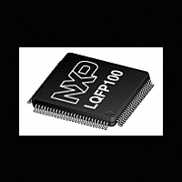
LPC2921_23_25 NXP Semiconductors, LPC2921_23_25 Datasheet - Page 43

LPC2921_23_25
Manufacturer Part Number
LPC2921_23_25
Description
The LPC2921/2923/2925 combine an ARM968E-S CPU core with two integrated TCMblocks operating at frequencies of up to 125 MHz, Full-speed USB 2
Manufacturer
NXP Semiconductors
Datasheet
1.LPC2921_23_25.pdf
(84 pages)
- Current page: 43 of 84
- Download datasheet (552Kb)
NXP Semiconductors
LPC2921_23_25_3
Product data sheet
Fig 9.
CLOCK GENERATION UNIT (CGU0)
400 kHz LP_OSC
Block diagram of the CGU0 (see
OSCILLATOR
EXTERNAL
FREQUENCY
MONITOR
There are two primary clock generators: a low-power ring oscillator (LP_OSC) and a
crystal oscillator. See
LP_OSC is the source for the BASE_PCR_CLK that clocks the CGU itself and for
BASE_SAFE_CLK that clocks a minimum of other logic in the device (like the watchdog
timer). To prevent the device from losing its clock source LP_OSC cannot be put into
power-down. The crystal oscillator can be used as source for high-frequency clocks or as
an external clock input if a crystal is not connected.
Secondary clock generators are a PLL and seven fractional dividers (FDIV[0:6]). The PLL
has three clock outputs: normal, 120° phase-shifted and 240° phase-shifted.
PLL
clkout
clkout120
clkout240
DETECTION
CLOCK
All information provided in this document is subject to legal disclaimers.
Table 24
Figure
Rev. 03 — 14 April 2010
AHB TO DTL BRIDGE
for all base clocks)
9.
FDIV0
FDIV1
FDIV6
ARM9 microcontroller with CAN, LIN, and USB
LPC2921/2923/2925
OUT 0
OUT 1
OUT 2
OUT 3
OUT 11
002aae147
© NXP B.V. 2010. All rights reserved.
BASE_SAFE_CLK
BASE_SYS_CLK
BASE_PCR_CLK
BASE_IVNSS_CLK
BASE_ICLK1_CLK
43 of 84
Related parts for LPC2921_23_25
Image
Part Number
Description
Manufacturer
Datasheet
Request
R
Part Number:
Description:
Arm9 Microcontroller With Can, Lin, And Usb Device
Manufacturer:
NXP Semiconductors
Datasheet:
Part Number:
Description:
(LPC2921 - LPC2925) ARM9 microcontroller
Manufacturer:
NXP Semiconductors
Datasheet:
Part Number:
Description:
NXP Semiconductors designed the LPC2420/2460 microcontroller around a 16-bit/32-bitARM7TDMI-S CPU core with real-time debug interfaces that include both JTAG andembedded trace
Manufacturer:
NXP Semiconductors
Datasheet:

Part Number:
Description:
NXP Semiconductors designed the LPC2458 microcontroller around a 16-bit/32-bitARM7TDMI-S CPU core with real-time debug interfaces that include both JTAG andembedded trace
Manufacturer:
NXP Semiconductors
Datasheet:
Part Number:
Description:
NXP Semiconductors designed the LPC2468 microcontroller around a 16-bit/32-bitARM7TDMI-S CPU core with real-time debug interfaces that include both JTAG andembedded trace
Manufacturer:
NXP Semiconductors
Datasheet:
Part Number:
Description:
NXP Semiconductors designed the LPC2470 microcontroller, powered by theARM7TDMI-S core, to be a highly integrated microcontroller for a wide range ofapplications that require advanced communications and high quality graphic displays
Manufacturer:
NXP Semiconductors
Datasheet:
Part Number:
Description:
NXP Semiconductors designed the LPC2478 microcontroller, powered by theARM7TDMI-S core, to be a highly integrated microcontroller for a wide range ofapplications that require advanced communications and high quality graphic displays
Manufacturer:
NXP Semiconductors
Datasheet:
Part Number:
Description:
The Philips Semiconductors XA (eXtended Architecture) family of 16-bit single-chip microcontrollers is powerful enough to easily handle the requirements of high performance embedded applications, yet inexpensive enough to compete in the market for hi
Manufacturer:
NXP Semiconductors
Datasheet:
Part Number:
Description:
The XA-S3 device is a member of Philips Semiconductors? XA(eXtended Architecture) family of high performance 16-bitsingle-chip microcontrollers
Manufacturer:
NXP Semiconductors
Datasheet:

Part Number:
Description:
The NXP BlueStreak LH75401/LH75411 family consists of two low-cost 16/32-bit System-on-Chip (SoC) devices
Manufacturer:
NXP Semiconductors
Datasheet:

Part Number:
Description:
The NXP LPC3130/3131 combine an 180 MHz ARM926EJ-S CPU core, high-speed USB2
Manufacturer:
NXP Semiconductors
Datasheet:

Part Number:
Description:
The NXP LPC3141 combine a 270 MHz ARM926EJ-S CPU core, High-speed USB 2
Manufacturer:
NXP Semiconductors

Part Number:
Description:
The NXP LPC3143 combine a 270 MHz ARM926EJ-S CPU core, High-speed USB 2
Manufacturer:
NXP Semiconductors

Part Number:
Description:
The NXP LPC3152 combines an 180 MHz ARM926EJ-S CPU core, High-speed USB 2
Manufacturer:
NXP Semiconductors


