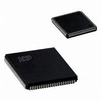
SC28L198A1A,518 NXP Semiconductors, SC28L198A1A,518 Datasheet - Page 50

SC28L198A1A,518
Manufacturer Part Number
SC28L198A1A,518
Description
IC UART OCTAL SOT189-3
Manufacturer
NXP Semiconductors
Type
Octal UART for 3.3 V and 5 V supply voltager
Datasheet
1.SC28L198A1BE557.pdf
(57 pages)
Specifications of SC28L198A1A,518
Number Of Channels
8
Package / Case
84-LCC (J-Lead)
Features
False-start Bit Detection
Fifo's
16 Byte
Voltage - Supply
3.3V, 5V
With Auto Flow Control
Yes
With False Start Bit Detection
Yes
With Modem Control
Yes
With Cmos
Yes
Mounting Type
Surface Mount
Data Rate
0.4608 MBd
Supply Voltage (max)
5.5 V
Supply Voltage (min)
3 V
Supply Current
150 mA
Maximum Operating Temperature
+ 85 C
Minimum Operating Temperature
- 40 C
Mounting Style
SMD/SMT
Operating Supply Voltage
3.3 V or 5 V
Transmit Fifo
16Byte
Receive Fifo
16Byte
Transmitter And Receiver Fifo Counter
No
Operating Supply Voltage (typ)
3.3/5V
Package Type
PLCC
Operating Supply Voltage (max)
5.5V
Operating Supply Voltage (min)
3V
Mounting
Surface Mount
Operating Temperature (min)
-40C
Operating Temperature (max)
85C
Operating Temperature Classification
Industrial
Lead Free Status / RoHS Status
Lead free / RoHS Compliant
Lead Free Status / RoHS Status
Lead free / RoHS Compliant, Lead free / RoHS Compliant
Other names
935261323518
SC28L198A1A-T
SC28L198A1A-T
SC28L198A1A-T
SC28L198A1A-T
Philips Semiconductors
2006 Aug 10
NOTES:
C1 and C2 should be based on manufacturer’s specification.
X1 and X2 parasitic capacitance IS 1-2pF AND 3-5pF, respectively.
GAIN:
PHASE: at 4MHz 272 to 276 ; at 8MHz 272 to 276
The above figures for 5V operation. Operation at 3V is to be determined.
Octal UART for 3.3 V and 5 V supply voltage
NOTE: CEN must not be active during an IACKN cycle. If CEN is active, IACKN will be ignored
C1 and C2 should be chosen according to the
crystal manufacturer’s specification.
C1 and C2 values will include any parasitic
capacitance of the wiring.
ADDRESS
DACKN
IACKN
W_RN
SCLK
DATA
CEN
at 4MHz 8 to 14db; at 8MHz 2 to 6db
and a normal read or write will be executed according to W_RN. In the synchronous
mode, extended IACKN signal will start another IACKN. (This may not be desired, but
is allowed.)
T/R f
INVALID
X1
C1 = C2 = 24pF FOR C
C1
C2
t
CS
3.6864MHz
C1
L
INVALID
= 20PF
Figure 7. X1/X2 Communication Crystal Clock
Figure 6. Basic IACKN Cycle, ASYNC/SYNC
f
X1
t
RWS
X1 L/H
X1
X2
C2
DON’T CARE
DON’T CARE
28C198
50
FREQUENCY:
LOAD CAPACITANCE (C
TYPE OF OPERATION:
4pF
3pF
t
AS
50 KOHMs
TO
150 KOHMs
C3
t
AH
t
DD
L
TYPICAL CRYSTAL SPECIFICATION
):
TO I/O CHANGE-OF-STATE DETECTORS
DAK
2 – 4MHZ
12 – 32pF
PARALLEL RESONANT, FUNDAMENTAL MODE
C4
C4
DLY
VALID
+5V
2
1K required for
38.4kHz CLOCK
NC
BRG
TTL gate.
DAK
CEN
HIGH
INVALID
DLY
t
DF
MUX
SC28L198
22
Product data sheet
INVALID
SD00525
STANDARD
BAUD
RATES
X1
X2
To
remainder
of circuit
SD00198


