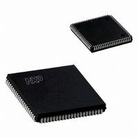
SC28L198A1A,518 NXP Semiconductors, SC28L198A1A,518 Datasheet - Page 42

SC28L198A1A,518
Manufacturer Part Number
SC28L198A1A,518
Description
IC UART OCTAL SOT189-3
Manufacturer
NXP Semiconductors
Type
Octal UART for 3.3 V and 5 V supply voltager
Datasheet
1.SC28L198A1BE557.pdf
(57 pages)
Specifications of SC28L198A1A,518
Number Of Channels
8
Package / Case
84-LCC (J-Lead)
Features
False-start Bit Detection
Fifo's
16 Byte
Voltage - Supply
3.3V, 5V
With Auto Flow Control
Yes
With False Start Bit Detection
Yes
With Modem Control
Yes
With Cmos
Yes
Mounting Type
Surface Mount
Data Rate
0.4608 MBd
Supply Voltage (max)
5.5 V
Supply Voltage (min)
3 V
Supply Current
150 mA
Maximum Operating Temperature
+ 85 C
Minimum Operating Temperature
- 40 C
Mounting Style
SMD/SMT
Operating Supply Voltage
3.3 V or 5 V
Transmit Fifo
16Byte
Receive Fifo
16Byte
Transmitter And Receiver Fifo Counter
No
Operating Supply Voltage (typ)
3.3/5V
Package Type
PLCC
Operating Supply Voltage (max)
5.5V
Operating Supply Voltage (min)
3V
Mounting
Surface Mount
Operating Temperature (min)
-40C
Operating Temperature (max)
85C
Operating Temperature Classification
Industrial
Lead Free Status / RoHS Status
Lead free / RoHS Compliant
Lead Free Status / RoHS Status
Lead free / RoHS Compliant, Lead free / RoHS Compliant
Other names
935261323518
SC28L198A1A-T
SC28L198A1A-T
SC28L198A1A-T
SC28L198A1A-T
1. Typical values are at +25 C, typical supply voltage and typical processing parameters.
2. All voltage measurements are referenced to V
3. Test conditions for itnerrupt and I/O outputs: CL = 50 pF. Test conditions for the rest of the outputs: CL = 60 pF.
4. Simultaneous switching more than 6 I/O port pins from 5 volts to 0 volts at full capacitive load may ground bounce on the output pins up to
5. All R
Philips Semiconductors
DC ELECTRICAL SPECIFICATIONS FOR COMMERCIAL AND INDUSTRIAL (5V)
V
NOTES:
2006 Aug 10
V
V
V
V
V
V
I
I
I
I
I
I
I
I
I
I
CC
IL
IH
L
ILCKX1
IHCKX1
OZH
OZL
ODL
ODH
CC
IL
IH
IH
OL
OH
OL
Octal UART for 3.3 V and 5 V supply voltage
SYMBOL
maximum. For X1/CLK this swing is between 0.4 V and 4.4 V. all time measurements are referenced at input voltages of V
appropriate.
0.95 volts.
= 5.0 volts
3
3
X
, T
X
, Brg Timer, I/O pins operating at 16 MHz. Sclk at 35 MHz and V
Input low voltage
Input high voltage (except X1/CLK)
Input high voltage (X1/CLK)
Output low voltage
Output high voltage (except OD outputs)
Open Drain low voltage
Input current low, I/O pins
Input current high, I/O pins
Input leakage current
X1/CLK input low current
X1/CLK input high current
Output off current high, 3–state data bus
Output off current low, 3–state data bus
Open–drain output low current in off state
Open drain output high current in off state
Power supply current
Operating mode 33 MHz
Static Power down (No clocks, Open–drains off,
inputs at V
10%; T
A
= –40 C to +85 C; unless otherwise specified
SS
or V
2
CC
PARAMETER
4
)
SS
. For testing, all inputs swing between 0.4 V and 2.4 V with a transition time of 10 ns
42
I
I
I
I
V
Vi
V
V
VIN=Vcc, X2=Open
V
V
V
V
TTL Input levels
CMOS input levels
CMOS input levels
OH
OH
OL
OL
IN
IN
IN
IN
IN
IN
IN
N
=Vss,X2=Open
= –400 A
= –100 A
= 0
= Vcc
= 0 to Vcc
= V
= 0
= 0
= V
= 4.0mA
= 14.0 mA
CONDITIONS
CC
CC
CC
at 5.6 volts. A worst–case environment.
TEST
0.8V
0.8V
0.9V
–450
MIN
V
–10
–10
–10
2.0
–5
SS
CC
CC
CC
LIMITS
<0.25
TYP
0.15
<0.1
<0.1
100
<.1
<.1
<.1
<.1
0.6
<1
26
1
SC28L198
MAX
Vcc
Vcc
450
150
0.8
0.4
0.4
Product data sheet
10
10
10
40
5
5
IL
and V
IH
UNIT
mA
mA
as
V
V
V
A
A
A
A
A
A
A


