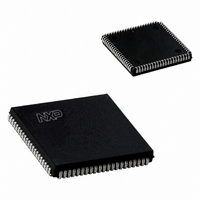
SC28L198A1A,518 NXP Semiconductors, SC28L198A1A,518 Datasheet - Page 29

SC28L198A1A,518
Manufacturer Part Number
SC28L198A1A,518
Description
IC UART OCTAL SOT189-3
Manufacturer
NXP Semiconductors
Type
Octal UART for 3.3 V and 5 V supply voltager
Datasheet
1.SC28L198A1BE557.pdf
(57 pages)
Specifications of SC28L198A1A,518
Number Of Channels
8
Package / Case
84-LCC (J-Lead)
Features
False-start Bit Detection
Fifo's
16 Byte
Voltage - Supply
3.3V, 5V
With Auto Flow Control
Yes
With False Start Bit Detection
Yes
With Modem Control
Yes
With Cmos
Yes
Mounting Type
Surface Mount
Data Rate
0.4608 MBd
Supply Voltage (max)
5.5 V
Supply Voltage (min)
3 V
Supply Current
150 mA
Maximum Operating Temperature
+ 85 C
Minimum Operating Temperature
- 40 C
Mounting Style
SMD/SMT
Operating Supply Voltage
3.3 V or 5 V
Transmit Fifo
16Byte
Receive Fifo
16Byte
Transmitter And Receiver Fifo Counter
No
Operating Supply Voltage (typ)
3.3/5V
Package Type
PLCC
Operating Supply Voltage (max)
5.5V
Operating Supply Voltage (min)
3V
Mounting
Surface Mount
Operating Temperature (min)
-40C
Operating Temperature (max)
85C
Operating Temperature Classification
Industrial
Lead Free Status / RoHS Status
Lead free / RoHS Compliant
Lead Free Status / RoHS Status
Lead free / RoHS Compliant, Lead free / RoHS Compliant
Other names
935261323518
SC28L198A1A-T
SC28L198A1A-T
SC28L198A1A-T
SC28L198A1A-T
Philips Semiconductors
Table 32. GIBCR – Global Interrupting Byte Count
Table 33. Global Interrupting Type Register
A register associated with the interrupting channel as defined in the
CIR. It contains the type of interrupt code for all interrupts.
Table 34. GRxFIFO – Global RxFIFO Register
The RxFIFO of the channel indicated in the CIR channel field.
Undefined when the CIR interrupt context is not a receiver interrupt.
Global TxFIFO Register
Table 36. IPR – Input Port Register,
This register may be read to determine the current level of the I/O
pins and examine the output of the change detectors assigned to
Table 37. I/OPIOR – I/O Port Interrupt and Output Register
I/OPIOR[7:4] bits activate the input change of state detectors. If a
pin is configured as an output, a b’1 value written to a I/O field has
no effect.
2006 Aug 10
Bits 7:4
Reserved
Bit 7:6
Receiver Interrupt
0x – not receiver
10 – with receive errors
11 – w/o receive errors
Bits 7:0
8 data bits of RxFIFO. MSBs set to 0 for 7, 6, 5 bit data
Bit 7
I/O3
change
0 – no change
1 – change
Bit 7
I/O3 enable
0 – disable
1 – enable
Octal UART for 3.3 V and 5 V supply voltage
Register
Bit 6
I/O2 enable
0 – disable
1 – enable
Bits 3:0
Channel byte count code
0000 = 1 AND RxRDY status set for RxFIFO
0000 = 1 AND TxRDY status set for TxD
0001 = 2
0010 = 3
.
1111 = 16
Bit 6
I/O2
change
0 – no change
1 – change
Bit 5
Transmitter Interrupt
0 – not transmitter
1 – transmitter interrupt
Bit 5
I/O1 enable
0 – disable
1 – enable
Bit 7
I/O1
change
0 – no change
1 – change
Bit 4
I/O0 enable
0 – disable
1 – enable
29
Bit 4:3
Reserved
read b’00
Bit 6
I/O0
change
0 – no change
1 – change
A register associated with the interrupting channel as defined in the
CIR. Its numerical value equals
the number of bytes minus 1 (count – 1) ready for transfer to the
transmitter or transfer from the receiver. It is undefined for other
types of interrupts
Table 35. GTxFIFO – Global TxFIFO Register
The TxFIFO of the channel indicated in the CIR channel field.
Undefined when the CIR interrupt context is not a transmitter
interrupt. Writing to the GTxFIFO when the current interrupt is not a
transmitter event may result in the characters being transmitted on a
different channel than intended.
each pin. If the change detection is not enabled or if the pin is
configured as an output, the associated change field will read b’0.
I/OPIOR[3:0] bits hold the datum which is the inverse of the datum
driven to its associated I/O pin when the I/OPCR control bits for that
pin are programmed to b’01.
Bits 7:0
8 data bits of TxFIFO. MSBs not used for 7, 6, 5 bit data
Bit 3
I/O3 output
OPR[3]
Bit 2
I/O2 output
OPR[2]
Bit 3
I/O3
state
The actual logic level at the I/O pin.
1 = high level; 0 =– low level.
Bit 2:0
Other types
000 – not ”other” type
001 – Change of State
010 – Address Recognition
Event
011 – Xon/Xoff status
100 – Not used
101 – Break Change
11x – do not occur
Bit 2
I/O2
state
Bit 1
I/O1 output
OPR[1]
Bit 1
I/O1
state
SC28L198
Product data sheet
Bit 0
I/O0 output
OPR[0]
Bit 0
I/O0
state


