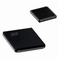
SC28L198A1A,518 NXP Semiconductors, SC28L198A1A,518 Datasheet - Page 46

SC28L198A1A,518
Manufacturer Part Number
SC28L198A1A,518
Description
IC UART OCTAL SOT189-3
Manufacturer
NXP Semiconductors
Type
Octal UART for 3.3 V and 5 V supply voltager
Datasheet
1.SC28L198A1BE557.pdf
(57 pages)
Specifications of SC28L198A1A,518
Number Of Channels
8
Package / Case
84-LCC (J-Lead)
Features
False-start Bit Detection
Fifo's
16 Byte
Voltage - Supply
3.3V, 5V
With Auto Flow Control
Yes
With False Start Bit Detection
Yes
With Modem Control
Yes
With Cmos
Yes
Mounting Type
Surface Mount
Data Rate
0.4608 MBd
Supply Voltage (max)
5.5 V
Supply Voltage (min)
3 V
Supply Current
150 mA
Maximum Operating Temperature
+ 85 C
Minimum Operating Temperature
- 40 C
Mounting Style
SMD/SMT
Operating Supply Voltage
3.3 V or 5 V
Transmit Fifo
16Byte
Receive Fifo
16Byte
Transmitter And Receiver Fifo Counter
No
Operating Supply Voltage (typ)
3.3/5V
Package Type
PLCC
Operating Supply Voltage (max)
5.5V
Operating Supply Voltage (min)
3V
Mounting
Surface Mount
Operating Temperature (min)
-40C
Operating Temperature (max)
85C
Operating Temperature Classification
Industrial
Lead Free Status / RoHS Status
Lead free / RoHS Compliant
Lead Free Status / RoHS Status
Lead free / RoHS Compliant, Lead free / RoHS Compliant
Other names
935261323518
SC28L198A1A-T
SC28L198A1A-T
SC28L198A1A-T
SC28L198A1A-T
Philips Semiconductors
AC ELECTRICAL CHARACTERISTICS FOR COMMERCIAL AND INDUSTRIAL (3.3 V)
V
2006 Aug 10
Reset Timing
t
Bus Timing
t
t
t
t
t
t
t
t
t
t
t
t
t
t
t
I/O Port Pin Timing
t
t
t
Interrupt Timing
t
t
Tx / Rx Clock Timing, External
t
f
t
f
Transmitter Timing
t
t
Receiver Timing
t
t
ts
Sclk Timing
t
t
CC
RES
AS
AH
CS
CS
CH
CH
STP
RWS
RWH
DD
DF
DF
DS
DH
RWD
PS
PH
PD
IR
DD
RX
RX
TX
TX
TXD
TCS
RXS
RXH
SCLKL
SCLKH
SYMBOL
SYMBOL
Octal UART for 3.3 V and 5 V supply voltage
STRT
4
4
= 3.3 volts
1
FIGURE
FIGURE
10%; T
A
RESET pulse width
A0-A7 setup time before Sclk C3 rising edge
A0-A7 hold time after Sclk C3 rising edge
CEN setup time before Sclk C1 high (ASYNC)
CEN setup time before Sclk C2 high (SYNC)
CEN hold time after Sclk C3 high (SYNC)
CEN hold time after Sclk C4 high (ASYNC)
Cen high befoe next C2 to stop next cycle (Sync Mode)
W-Rn setup time before Sclk C2 rising edge
W-Rn hold time after Sclk C3 rising edge
Read cycle Data valid after Sclk C3 falling edge
Read cycle data bus floating after CEN high (ASYNC)
Read cycle data bus floating after C4 end (SYNC)
Write cycle data setup time before Sclk C4 rising edge
Write cycle data hold time after Sclk C4 rising edge
High time between CEN low (ASYNC)
I/O input setup time before Sclk C3 falling edge (Read IPR)
I/O input hold time after Sclk C4 rising edge (Read IPR)
I/O output valid from:
Write Sclk C4 rising edge (write to I/OPIOR)
IRQN from:
Interrupt vector valid after C3 rising edge
RxC high or low time
RxC frequency (16 X)
TxC high or low time
TxC frequency (16 X)
TxD output delay from TxC low
TxC output delay from TxD output data
RxD data setup time to RxC high (data)
RxD data hold time from RxC high (data)
RxD data low time to for receiving a valid Start Bit
Min low time at Vil (0.8V)
Min high time at Vih (2.0V)
Internal interrupt source active bid
Software reset to IRQN inactive
Write IMR (set or clear IMR bit))
= –40 C to +85 C; unless otherwise specified
(1 X)
(1 X)
PARAMETER
PARAMETER
3
to IRQN inactive
46
2
MIN
-15
10
22
30
25
50
30
25
25
25
15
18
12
22
25
20
25
25
15
15
8
8
7
0
0
0
0
17
32
1
1
1
LIMITS
TYP
12
20
17
11
14
14
50
26
60
40
20
50
14
14
10
10
Sclk
3
3
3
4
4
8
7
4
Sclk
Sclk
Sclk
MAX
8.0
40
30
20
80
43
90
60
30
90
15
SC28L198
8
1
1
Product data sheet
bit time
UNIT
UNIT
MHz
MHz
MHz
Sclk
Sclk
ns
ns
ns
ns
ns
ns
ns
ns
ns
ns
ns
ns
ns
ns
ns
ns
ns
ns
ns
ns
ns
ns
ns
ns
ns
ns
ns
ns
ns


