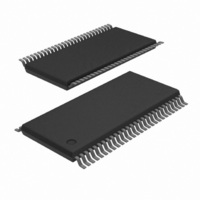
SC28L202A1DGG/G:11 NXP Semiconductors, SC28L202A1DGG/G:11 Datasheet - Page 52

SC28L202A1DGG/G:11
Manufacturer Part Number
SC28L202A1DGG/G:11
Description
IC UART DUAL W/FIFO 56-TSSOP
Manufacturer
NXP Semiconductors
Series
IMPACTr
Datasheet
1.SC28L202A1DGG118.pdf
(77 pages)
Specifications of SC28L202A1DGG/G:11
Features
False-start Bit Detection
Number Of Channels
2, DUART
Fifo's
256 Byte
Voltage - Supply
3.3V, 5V
With Parallel Port
Yes
With Auto Flow Control
Yes
With False Start Bit Detection
Yes
With Modem Control
Yes
With Cmos
Yes
Mounting Type
Surface Mount
Package / Case
56-TFSOP (0.240", 6.10mm Width)
Lead Free Status / RoHS Status
Lead free / RoHS Compliant
Other names
935279792112
SC28L202A1DGG/G
SC28L202A1DGG/G
SC28L202A1DGG/G
SC28L202A1DGG/G
Philips Semiconductors
IPCR Input Port Configuration Register
IPCR [7:4] I/03A, I/O2 A, I/O1 A, I/O0 A Change–of–State
These bits are set when a change–of–state, as defined in the input
port section of this data sheet, occurs at the respective input pins.
They are cleared when the IPCR is read by the CPU. A read of
the IPCR also clears ISR [7], the input change bit in the interrupt
status register. The setting of these bits can be programmed to
generate an interrupt to the CPU.
ACR Auxiliary Control Register
ACR[7] – Baud Rate Generator Set Select
This bit selects one of two sets of baud rates to be generated by the
BRG and it effects both channels. (see Table 13).
ACR[6:4] – Counter/Timer Mode And Clock Source Select
This field selects the operating mode of the counter/timer and its
clock source as shown in Table 14.
ACR[3:0] – I/O3 A, I/O2 A, I/O1 A, I/O0 A Change-of-State
Interrupt Enable
This field selects which bits of the input port change register (IPCR)
cause the input change bit in the interrupt status register (ISR [7]) to
be set. If a bit is in the ‘on’ state the setting of the corresponding bit
in the IPCR will also result in the setting of ISR[7], which results in
the generation of an interrupt output if IMR[7] = 1. If a bit is in the
‘off’ state, the setting of that bit in the IPCR has no effect on ISR[7].
2005 Nov 01
IPCR
ACR
Dual UART
Bit 7
Delta
I/O 3A
0 = no change
1 = change
Bit 7
BRG SET
Select
0 = set 1
1 = set 2
BIT 6
Counter Timer Mode
and
clock source select
See Table 14
BIT 6
Delta
I/O 2A
0 = no change
1 = change
BIT 5
BIT 5
Delta
I/O 1A
0 = no change
1 = change
BIT 4
BIT 3
Delta
I/O3 A interrupt
enable
0 = off
1 = enabled
46
BIT 4
Delta
I/O 0A
0 = no change
1 = change
IPCR [3:0] I/O3 A, I/O2 A, I/O1 A, I/O0 A logical level of I/O pin.
These bits provide the current state of the respective inputs. The
information is unlatched and reflects the state of the input pins at the
time the IPCR is read.
Table 14. ACR 6:4 Field Definition
ACR(6:4)
000
001
010
011
100
101
110
111
NOTE: The timer mode generates a square wave.
BIT 2
Delta
I/O2 A interrupt
enable
0 = off
1 = enabled
MODE
Counter
Counter
Counter
Counter
Timer
Timer
Timer
Timer
BIT 3
I/O 3A
0 = low
1 = High
CLOCK SOURCE
External (I/02A)
TxC A – 1X clock of Channel A
transmitter
TxC B – 1X clock of Channel B
transmitter
External (I/O 2A)
External (I/O2 A) divided by 16
Crystal or external clock (X1/Sclk)
(X1/Sclk) clock divided by 16
(X1/Sclk) clock divided by 16
BIT 2
I/O 2A
0 = low
1 = High
BIT 1
Delta
I/O1 A interrupt
enable
0 = off
1 = enabled
BIT 1
I/O 1A
0 = low
1 = High
SC28L202
BIT 0
Delta
I/O0 A interrupt
enable
0 = off
1 = enabled
Product data sheet
BIT 0
I/O 0A
0 = low
1 = High


