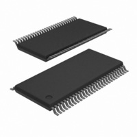
SC28L202A1DGG/G:11 NXP Semiconductors, SC28L202A1DGG/G:11 Datasheet - Page 45

SC28L202A1DGG/G:11
Manufacturer Part Number
SC28L202A1DGG/G:11
Description
IC UART DUAL W/FIFO 56-TSSOP
Manufacturer
NXP Semiconductors
Series
IMPACTr
Datasheet
1.SC28L202A1DGG118.pdf
(77 pages)
Specifications of SC28L202A1DGG/G:11
Features
False-start Bit Detection
Number Of Channels
2, DUART
Fifo's
256 Byte
Voltage - Supply
3.3V, 5V
With Parallel Port
Yes
With Auto Flow Control
Yes
With False Start Bit Detection
Yes
With Modem Control
Yes
With Cmos
Yes
Mounting Type
Surface Mount
Package / Case
56-TFSOP (0.240", 6.10mm Width)
Lead Free Status / RoHS Status
Lead free / RoHS Compliant
Other names
935279792112
SC28L202A1DGG/G
SC28L202A1DGG/G
SC28L202A1DGG/G
SC28L202A1DGG/G
Philips Semiconductors
THE REGISTERS FOR COMPATIBILITY WITH PREVIOUS DUARTS
The purpose of including previous functionality is to allow users to
call communications code that may be used in former systems.
When the registers in this lower 16–position address space is used
it will revoke programming done in the upper address space where
the addresses are duplicated. If functions have been called from
upper address space that DO NOT exist in the lower address space
they will remain active. It is therefore recommended that the ‘Reset
Table 7. SC28L92 Register Addressing READ (RDN = 0) WRITE (WRN = 0)
NOTE: The three MR Registers are accessed via the MR Pointer and Commands 0x1n and 0xBn (where n = represents receiver and
transmitter enable bits)
2005 Nov 01
Address
0
0
0
0
0
0
0
0
1
1
1
1
1
1
1
1
The following registers are unique for each Channel
Mode Register
Status Register
Clock
Select
Command
Register
Receiver
FIFO
Transmitter
FIFO
Dual UART
0
0
0
0
1
1
1
1
0
0
0
0
1
1
1
1
0
0
1
1
0
0
1
1
0
0
1
1
0
0
1
1
0
1
0
1
0
1
0
1
0
1
0
1
0
1
0
1
READ (RDN = 0)
Mode Register A (MR0 A, MR1 A, MR2 A)
Status Register A (SR A)
Reserved
Rx Holding Register A (RxFIFO A)
Input Port Change Register (IPCR)
Interrupt Status Register (ISR)
Counter/Timer Upper (CTPU)
Counter/Timer Lower (CTPL)
Mode Register B (MR0 B, MR1 B, MR2 B)
Status Register B (SR B)
Reserved
Rx Holding Register B (RxFIFO B)
IVR or general purpose register
Input Port (IPR) I/O(6:0) A
Start Counter Command (C/T 0)
Stop Counter Command (C/T 0)
MRn A
SR A
CSR A
CR A
RxFIFO A
TxFIFO A
MRn B
SR B
CSR B
CR B
RxFIFO B
TxFIFO B
R/W
R only
W only
W only
R only
W only
39
WRITE (WRN = 0)
Mode Register A (MR0 A, MR1 A, MR2 A)
Clock Select Register A (CSR A )
Command Register A (CR A)
Tx Holding Register A (TxFIFO A)
Aux. Control Register (ACR)
Interrupt Mask Register (IMR)
C/T Upper Preset Register (CTPU)
C/T Lower Preset Register (CTPL)
Mode Register B (MR0 B, MR1 B, MR2 B)
Clock Select Register B (CSR B )
Command Register B (CR B)
Tx Holding Register B (TxFIFO B)
IVR or general purpose register
Output Port Confide. Register (OPCR) I/O(7:2) B
Set Output Port Bits Command (SOPR) I/O(7:0) B
Reset output Port Bits Command (ROPR) I/O(7:0) B
to C92’ command be issued before calling code written for older
devices. This is just recommended. If one wishes to enhance
previous code by using Xon/Xoff, for example, there is no restriction
against it. These registers provide the original functionality of
previous Philips DUARTs: SCN2681, SCN68681, SCC2691,
SCC68692, SC26C92 and SC28L92.
These registers support functions for both Channels
Input Port Change Register
Auxiliary Control Register
Interrupt Status Register
Interrupt Mask Register
Counter Timer Upper Value
Counter Timer Lower Value
Counter Timer Preset Upper
Counter Timer Preset Lower
Input Port Register
Output Configuration Register
Set Output Port
Reset Output Port
IPCR
ACR
ISR
IMR
CTPU
CTPL
CTPU
CTPL
IPR
OPCR
Bits
Bits
SC28L202
Product data sheet
R
W
R
W
R
R
W
W
R
W
W
W


