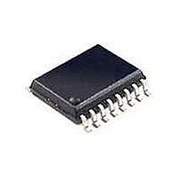
SI3050-KT Silicon Laboratories Inc, SI3050-KT Datasheet - Page 9

SI3050-KT
Manufacturer Part Number
SI3050-KT
Description
IC VOICE DAA GCI/PCM/SPI 20TSSOP
Manufacturer
Silicon Laboratories Inc
Type
Chipsetr
Specifications of SI3050-KT
Package / Case
20-TSSOP
Function
Data Access Arrangement (DAA)
Interface
PCM, Serial, SPI
Number Of Circuits
1
Voltage - Supply
3 V ~ 3.6 V
Current - Supply
8.5mA
Operating Temperature
0°C ~ 70°C
Mounting Type
Surface Mount
Includes
Line Voltage Monitor, Loop Current Monitor, Overload Detection, Parallel Handset Detection, Polarity Reversal Detection, TIP and
Product
Modem Chip
Supply Voltage (min)
3 V
Supply Current
8.5 mA
Maximum Operating Temperature
+ 70 C
Minimum Operating Temperature
0 C
Mounting Style
SMD/SMT
Lead Free Status / RoHS Status
Contains lead / RoHS non-compliant
Power (watts)
-
Lead Free Status / RoHS Status
Lead free / RoHS Compliant, Contains lead / RoHS non-compliant
Available stocks
Company
Part Number
Manufacturer
Quantity
Price
Part Number:
SI3050-KT
Manufacturer:
SILICONIX
Quantity:
20 000
Company:
Part Number:
SI3050-KTR
Manufacturer:
NEC
Quantity:
947
Part Number:
SI3050-KTR
Manufacturer:
SILICON LABS/芯科
Quantity:
20 000
Table 4. AC Characteristics (Continued)
(V
Table 5. Absolute Maximum Ratings
Transhybrid Balance
Transhybrid Balance
Two-Wire Return Loss
Two-Wire Return Loss
Notes:
Parameter
DC Supply Voltage
Input Current, Si3050 Digital Input Pins
Digital Input Voltage
Ambient Operating Temperature Range
Storage Temperature Range
Note: Permanent device damage can occur if the above Absolute Maximum Ratings are exceeded. Functional operation
Parameter
D
=
1. Measured at TIP and RING with 600 Ω termination at 1 kHz, as shown in Figure 1 on page 6.
2. The transmit and receive full scale level of +3.2 dBm can be achieved with a 600 Ω ac termination. While the transmit
3. Receive full scale level produces –0.9 dBFS at DTX.
4. DR
5. Measurement is 300 to 3400 Hz. Applies to both transmit and receive paths.
6. Vin
7. THD
8. DR
9. Refer to Tables 10–11 for relative gain accuracy characteristics (passband ripple).
3.0 to 3.6 V, T
and receive level in dBm varies with reference impedance, the DAA will transmit and receive 1 dBV into all reference
impedances.
above.
should be restricted to the conditions as specified in the operational sections of this data sheet. Exposure to absolute
maximum rating conditions for extended periods might affect device reliability.
CID
=
=
=
1 kHz, –3 dBFS.
20 x log (rms V
=
20 x log (rms distortion/rms signal).
20 x log (rms V
A
=
0 to 70 °C for K-Grade,
FS
/rms Vin) + 20 x log (rms V
CID
/rms V
Symbol
IN
) + 20 x log (rms V
Fs = 8000 Hz,
1 kHz, all ac terminations
Symbol
in
T
V
/rms noise). Here, V
Rev. 1.0
300–3.4 kHz, all ac
300–3.4 kHz, all ac
V
I
T
STG
IND
IN
D
A
Test Condition
IN
terminations
1 kHz, all ac
terminations
terminations
/rms noise). V
see
"Typical Application Schematic" on page 17
CID
–0.3 to (V
FS
is the 1.5 V full-scale level.
–0.5 to 3.6
–40 to 100
–65 to 150
is the 0 dBm full-scale level per Note 1
Value
±10
D
+ 0.3)
Min
20
25
—
—
Typ
30
32
—
—
Max
Si3050
—
—
—
—
Unit
mA
°C
°C
V
V
)
Unit
dB
dB
dB
dB
9


