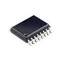
SI3050-KT Silicon Laboratories Inc, SI3050-KT Datasheet - Page 36

SI3050-KT
Manufacturer Part Number
SI3050-KT
Description
IC VOICE DAA GCI/PCM/SPI 20TSSOP
Manufacturer
Silicon Laboratories Inc
Type
Chipsetr
Specifications of SI3050-KT
Package / Case
20-TSSOP
Function
Data Access Arrangement (DAA)
Interface
PCM, Serial, SPI
Number Of Circuits
1
Voltage - Supply
3 V ~ 3.6 V
Current - Supply
8.5mA
Operating Temperature
0°C ~ 70°C
Mounting Type
Surface Mount
Includes
Line Voltage Monitor, Loop Current Monitor, Overload Detection, Parallel Handset Detection, Polarity Reversal Detection, TIP and
Product
Modem Chip
Supply Voltage (min)
3 V
Supply Current
8.5 mA
Maximum Operating Temperature
+ 70 C
Minimum Operating Temperature
0 C
Mounting Style
SMD/SMT
Lead Free Status / RoHS Status
Contains lead / RoHS non-compliant
Power (watts)
-
Lead Free Status / RoHS Status
Lead free / RoHS Compliant, Contains lead / RoHS non-compliant
Available stocks
Company
Part Number
Manufacturer
Quantity
Price
Part Number:
SI3050-KT
Manufacturer:
SILICONIX
Quantity:
20 000
Company:
Part Number:
SI3050-KTR
Manufacturer:
NEC
Quantity:
947
Part Number:
SI3050-KTR
Manufacturer:
SILICON LABS/芯科
Quantity:
20 000
Si3050
Transhybrid Balance
The Si3050 contains an on-chip analog hybrid that
performs the 2- to 4-wire conversion and near-end echo
cancellation. This hybrid circuit is adjusted for each ac
termination setting selected to achieve a minimum
transhybrid balance of 20 dB.
The Si3050 also offers a digital hybrid stage for
additional near-end echo cancellation. For each ac
termination setting, the eight programmable hybrid
registers (Registers 45–52) can be programmed with
coefficients to increase cancellation of real-world line
anomalies. This digital filter can produce 10 dB or
greater of near-end echo cancellation in addition to the
20 dB from the analog hybrid circuitry. See AN84 for a
more detailed description of the digital hybrid and how
to use it.
Filter Selection
The Si3050 supports additional filter selections for the
receive and transmit signals as defined in Tables 10 and
11. The IIRE bit (Register 16, bit 4) selects between the
IIR and FIR filters. The IIR filter provides a shorter, but
non-linear, group delay alternative to the default FIR
filter, and only operates with an 8 kHz sample rate. The
FILT bit (Register 31, bit 1) selects a –3 dB low
frequency pole of 5 Hz when cleared and a –3 dB low
frequency pole of 200 Hz (per EIA/TIA 464) when set.
The FILT bit affects the receive path only.
Clock Generation
The Si3050 generates the necessary internal clock
frequencies from the PCLK input. PCLK must be
synchronous to the 8 kHz FSYNC clock and run at one
of the following rates: 256 kHz, 512 kHz, 768 kHz,
1.024 MHz,
8.192 MHz. The ratio of the PCLK rate to the FSYNC
rate is determined internally by the DAA and is
transferred into internal registers after a reset. These
internal registers are not accessible through register
reads or writes. Figure 25 shows the operation of the
36
PCLK
1.53 MHz,
PFD
2.048 MHz,
Figure 27. PLL Clock Synthesizer
4.09 MHz,
Internal PLL
Register
DIV M
Rev. 1.0
or
Si3050 clock circuitry.
The PLL clock synthesizer settles quickly after powerup.
However, the settling time depends on the PCLK
frequency and it can be approximately predicted by the
following equation:
For all valid PCLK frequencies listed above, the default
line sample rate is 8 kHz. This sample rate can be
increased to 16 kHz by setting the HSSM bit
(Register 7, bit 3). Regardless of the sample rate
frequency, the serial data communication rate of the
PCM and GCI highways remains 8 kHz. When the
16 kHz sample rate is selected, additional timeslots in
the PCM or GCI highway are used to transfer the
additional data.
Communication Interface Mode Selection
The Si3050 supports two communication interface
protocols:
!
!
A pin-strapping method (specifically, the state of SCLK
on power-up [reset]) is used to select between the two
communication interface protocols. Tables 19 and 20
specify how to select a communication mode, and how
the various pins are used in each mode.
When operating in PCM/SPI mode, the GCI control
register should not be written (i.e., Register 42 must
each remain set at 0000_0000 when using the PCM/
SPI highway mode). Similarly, when operating in GCI
highway mode the PCM registers should not be written
(i.e., Registers 33–37 must remain set to 0000_0000
when using the GCI highway mode).
PCM/SPI mode where data and control information
transmission/reception occurs across separate
buses (PCM highway for data, and SPI port for
control).
GCI mode where data and control information is
multiplexed and transmission/reception occurs
across the GCI highway bus.
T
settle
VCO
= 64/F
PCLK
÷ 2
÷ 3
16.384 MHz


