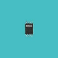
SI6933DQ Fairchild Semiconductor, SI6933DQ Datasheet - Page 2

SI6933DQ
Manufacturer Part Number
SI6933DQ
Description
MOSFET Small Signal 30V/25V PCh MOSFET Dual
Manufacturer
Fairchild Semiconductor
Datasheet
1.SI6933DQ.pdf
(5 pages)
Specifications of SI6933DQ
Configuration
Dual Dual Source
Transistor Polarity
P-Channel
Resistance Drain-source Rds (on)
28 m Ohms
Drain-source Breakdown Voltage
- 30 V
Gate-source Breakdown Voltage
+/- 20 V
Continuous Drain Current
- 3.5 A
Power Dissipation
1 W
Maximum Operating Temperature
+ 150 C
Mounting Style
SMD/SMT
Package / Case
TSSOP-8
Minimum Operating Temperature
- 55 C
Lead Free Status / Rohs Status
Details
Available stocks
Company
Part Number
Manufacturer
Quantity
Price
Part Number:
SI6933DQ
Manufacturer:
SILICONIX
Quantity:
20 000
Company:
Part Number:
SI6933DQ-T1-E3
Manufacturer:
VISHAY
Quantity:
2 500
Part Number:
SI6933DQ-T1-E3
Manufacturer:
VISHAY/Õ©üõĖ¢
Quantity:
20 000
Notes:
1. R
2. Pulse Test: Pulse Width < 300 s, Duty Cycle < 2.0%
Electrical Characteristics
Symbol
Off Characteristics
BV
I
I
I
On Characteristics
V
R
I
g
Dynamic Characteristics
C
C
C
Switching Characteristics
t
t
t
t
Q
Q
Q
Drain–Source Diode Characteristics and Maximum Ratings
I
V
the drain pins. R
a) R
b) R
d(on)
r
d(off)
f
DSS
GSSF
GSSR
D(on)
S
BV
V
FS
GS(th)
SD
DS(on)
iss
oss
rss
g
gs
gd
JA
GS(th)
DSS
T
T
is the sum of the junction-to-case and case-to-ambient thermal resistance where the case thermal reference is defined as the solder mounting surface of
DSS
J
J
JA
JA
is 100 C/W (steady state) when mounted on a 1 inch² copper pad on FR-4.
is 125 C/W (steady state) when mounted on a minimum copper pad on FR-4.
Drain–Source Breakdown Voltage
Breakdown Voltage Temperature
Coefficient
Zero Gate Voltage Drain Current
Gate–Body Leakage, Forward
Gate–Body Leakage, Reverse
Gate Threshold Voltage
Gate Threshold Voltage
Temperature Coefficient
Static Drain–Source
On–Resistance
On–State Drain Current
Forward Transconductance
Input Capacitance
Output Capacitance
Reverse Transfer Capacitance
Turn–On Delay Time
Turn–On Rise Time
Turn–Off Delay Time
Turn–Off Fall Time
Total Gate Charge
Gate–Source Charge
Gate–Drain Charge
Maximum Continuous Drain–Source Diode Forward Current
Drain–Source Diode Forward
Voltage
JC
is guaranteed by design while R
Parameter
(Note 2)
(Note 2)
CA
is determined by the user's board design.
V
I
V
V
V
V
I
V
V
V
V
V
V
f = 1.0 MHz
V
V
V
V
V
D
D
T
GS
DS
GS
GS
DS
GS
GS
GS
GS
DS
DS
DD
GS
DS
GS
GS
= –250 A, Referenced to 25 C
= –250 A, Referenced to 25 C
A
= 25°C unless otherwise noted
= –24 V,
= V
= –5 V,
= –15 V,
= –15 V,
= –10 V,
= –15V,
= –10 V
= 0 V,
= –20 V,
= 20 V,
= –10 V,
= –4.5 V,
= –10 V, I
= –10 V,
= 0 V,
Test Conditions
GS
,
I
S
D
= –0.83 A
= –3.5 A, T
I
V
V
V
I
I
I
V
I
V
I
D
D
D
D
D
I
R
D
D
GS
DS
DS
DS
GS
= –250 A
= –250 A
= –3.5 A
= –2.5 A
= –3.5 A
GEN
= –3.5 A,
= –1 A,
= 0 V
= 0 V
= 0 V
= –5 V
= 0 V,
= 6
(Note 2)
J
=125 C
Min
–30
–15
–1
Typ Max Units
–1.8
–0.7
–22
854
215
112
4.6
2.4
28
42
38
12
14
29
15
9
8
3
–0.83
–100
–1.2
100
–1
–3
45
85
54
20
20
60
20
30
Si6933DQ Rev. B (W)
mV/ C
mV/ C
m
nC
nC
nC
nA
nA
pF
pF
pF
ns
ns
ns
ns
V
V
A
S
A
V
A


