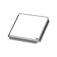
LPC2214FBD144 NXP Semiconductors, LPC2214FBD144 Datasheet - Page 7

LPC2214FBD144
Manufacturer Part Number
LPC2214FBD144
Description
Manufacturer
NXP Semiconductors
Datasheet
1.LPC2214FBD144.pdf
(45 pages)
Specifications of LPC2214FBD144
Cpu Family
LPC2000
Device Core
ARM7TDMI-S
Device Core Size
16/32Bit
Frequency (max)
60MHz
Interface Type
I2C/SPI
Program Memory Type
Flash
Program Memory Size
256KB
Total Internal Ram Size
16KB
# I/os (max)
112
Number Of Timers - General Purpose
2
Operating Supply Voltage (typ)
1.8/3.3V
Operating Supply Voltage (max)
1.95/3.6V
Operating Supply Voltage (min)
1.65/2.5/3V
On-chip Adc
8-chx10-bit
Instruction Set Architecture
RISC
Operating Temp Range
-40C to 85C
Operating Temperature Classification
Industrial
Mounting
Surface Mount
Pin Count
144
Package Type
LQFP
Lead Free Status / Rohs Status
Compliant
Available stocks
Company
Part Number
Manufacturer
Quantity
Price
Part Number:
LPC2214FBD144
Manufacturer:
NXP
Quantity:
20 000
Company:
Part Number:
LPC2214FBD144,551
Manufacturer:
NXP Semiconductors
Quantity:
10 000
Company:
Part Number:
LPC2214FBD144/01
Manufacturer:
LT
Quantity:
3 400
Company:
Part Number:
LPC2214FBD144/01
Manufacturer:
NXP
Quantity:
5 000
Part Number:
LPC2214FBD144/01
Manufacturer:
NXP/恩智浦
Quantity:
20 000
Company:
Part Number:
LPC2214FBD144/01,5
Manufacturer:
Intersil
Quantity:
637
Company:
Part Number:
LPC2214FBD144/01,5
Manufacturer:
NXP Semiconductors
Quantity:
10 000
Part Number:
LPC2214FBD144/01,5
Manufacturer:
NXP/恩智浦
Quantity:
20 000
Company:
Part Number:
LPC2214FBD144/015
Manufacturer:
NXP Semiconductors
Quantity:
135
NXP Semiconductors
Table 3.
LPC2212_2214_4
Product data sheet
Symbol
P0[14]/DCD1/EINT1
P0[15]/RI1/EINT2
P0[16]/EINT0/MAT0[2]/
CAP0[2]
P0[17]/CAP1[2]/SCK1/
MAT1[2]
P0[18]/CAP1[3]/MISO1/
MAT1[3]
P0[19]/MAT1[2]/MOSI1/
CAP1[2]
P0[20]/MAT1[3]/SSEL1/
EINT3
P0[21]/PWM5/CAP1[3]
P0[22]/CAP0[0]/MAT0[0] 5
P0[23]
P0[24]
P0[25]
P0[27]/AIN0/CAP0[1]/
MAT0[1]
P0[28]/AIN1/CAP0[2]/
MAT0[2]
P0[29]/AIN2/CAP0[3]/
MAT0[3]
Pin description
Pin
92
99
100
101
121
122
123
4
6
8
21
23
25
32
…continued
Type Description
I
I
I
I
I
O
I
I
I/O
O
I
I/O
O
O
I/O
I
O
I
I
O
I
I
O
I/O
I/O
I/O
I
I
O
I
I
O
I
I
O
DCD1 — Data Carrier Detect input for UART1.
EINT1 — External interrupt 1 input.
Note: LOW on this pin while RESET is LOW forces on-chip bootloader to take
over control of the part after reset.
RI1 — Ring Indicator input for UART1.
EINT2 — External interrupt 2 input.
EINT0 — External interrupt 0 input.
MAT0[2] — Match output for Timer 0, channel 2.
CAP0[2] — Capture input for Timer 0, channel 2.
CAP1[2] — Capture input for Timer 1, channel 2.
SCK1 — Serial Clock for SPI1/SSP
to slave.
MAT1[2] — Match output for Timer 1, channel 2.
CAP1[3] — Capture input for Timer 1, channel 3.
MISO1 — Master In Slave Out for SPI1/SSP
data output from SPI slave.
MAT1[3] — Match output for Timer 1, channel 3.
MAT1[2] — Match output for Timer 1, channel 2.
MOSI1 — Master Out Slave In for SPI1/SSP
or data input to SPI slave.
CAP1[2] — Capture input for Timer 1, channel 2.
MAT1[3] — Match output for Timer 1, channel 3.
SSEL1 — Slave Select for SPI1/SSP
EINT3 — External interrupt 3 input.
PWM5 — Pulse Width Modulator output 5.
CAP1[3] — Capture input for Timer 1, channel 3.
CAP0[0] — Capture input for Timer 0, channel 0.
MAT0[0] — Match output for Timer 0, channel 0.
General purpose bidirectional digital port only.
General purpose bidirectional digital port only.
General purpose bidirectional digital port only.
AIN0 — ADC, input 0. This analog input is always connected to its pin.
CAP0[1] — Capture input for Timer 0, channel 1.
MAT0[1] — Match output for Timer 0, channel 1.
AIN1 — ADC, input 1. This analog input is always connected to its pin.
CAP0[2] — Capture input for Timer 0, channel 2.
MAT0[2] — Match output for Timer 0, channel 2.
AIN2 — ADC, input 2. This analog input is always connected to its pin.
CAP0[3] — Capture input for Timer 0, Channel 3.
MAT0[3] — Match output for Timer 0, channel 3.
Rev. 04 — 3 January 2008
[1]
[1]
. SPI clock output from master or input
. Selects the SPI interface as a slave.
16/32-bit ARM microcontrollers
LPC2212/2214
[1]
[1]
. Data input to SPI master or
. Data output from SPI master
© NXP B.V. 2008. All rights reserved.
7 of 45


