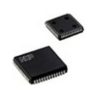
SC68C562C1A NXP Semiconductors, SC68C562C1A Datasheet - Page 8

SC68C562C1A
Manufacturer Part Number
SC68C562C1A
Description
Manufacturer
NXP Semiconductors
Datasheet
1.SC68C562C1A.pdf
(24 pages)
Specifications of SC68C562C1A
Operating Supply Voltage (typ)
5V
Operating Temp Range
0C to 70C
Operating Temperature Classification
Commercial
Package Type
PLCC
Mounting
Surface Mount
Pin Count
52
Lead Free Status / Rohs Status
Compliant
Available stocks
Company
Part Number
Manufacturer
Quantity
Price
Company:
Part Number:
SC68C562C1A
Manufacturer:
NXP
Quantity:
5 510
Company:
Part Number:
SC68C562C1A
Manufacturer:
ARK
Quantity:
5 510
1. Stresses above those listed under Absolute Maximum Ratings may cause permanent damage to the device. This is a stress rating only and
2. Clock may be stopped (DC) for testing purposes or when the CDUSCC is in non-operational modes. Operation down to 0 rate clocks is
3. This product includes circuitry specifically designed for the protection of its internal devices from damaging effects of excessive static
4. Parameters are valid over specified temperature and voltage range.
5. All voltage measurements are referenced to ground (GND). For testing, all inputs except X1/CLK swing between 0.2 V and 3.0 V with a
6. See Figure 18 for test conditions for outputs.
7. Tests for open drain outputs are intended to guarantee switching of the output transistor. To include noise margin this response is measured
8. Execution of the valid command (after it is latched) requires a minimum of three rising edges of X1 (see Figure 19).
9. These values were no explicitly tested; they are guaranteed by design and characterization data.
10. X1/CLK and X2 are not tested with a crystal installed.
11. X1/CLK frequency must be at least as fast as the faster of the receiver or transmitter data rate.
12. The X1 clock drives DTACKN, Baud Rate Generator, command register and the update of the FIFO fill level encoders. The Command
13. The 68562 bus interface may be operated in two modes; a 68000 compatible mode with automatic DTACK generation and a short chip
14. Also includes X2/IDCN pin in IDC mode.
15. In case of 3-state output, output levels V
16. V
Philips Semiconductors
ELECTRICAL CHARACTERISTICS
T
NOTES:
2004 Mar 29
amb
SYMBOL
SYMBOL
V
V
V
V
I
I
I
I
I
I
I
I
I
I
C
C
C
ILX1
IHX1
SCX2
IL
L
OZH
OZL
ODL
ODH
CC
IL
IH
OL
OH
CMOS Dual universal serial communications controller
(CDUSCC)
IN
OUT
I/O
functional operation of the device at these or any other conditions above those indicated in the operation section of this specification is not
implied.
implied by a full static CMOS design, but is not verified in testing or characterization.
charge. Nonetheless, it is suggested that conventional precautions be taken to avoid applying any voltages larger than the rated maxima.
transition time of 20 ns maximum. For X1/CLK, this swing is between 0.2 V and 4.4 V. All time measurements are referenced at input
voltages of 0.2 V and 3.0 V and output voltages of 0.8 V and 2.0 V, as appropriate.
from the switching signal midpoint to 0.2 V above the required output level.
Register requires three X1 clocks between two commands; FIFO fill level encoding requires 2.5 to 3.5 X1 cycles.
select mode. DTACKN should not be used externally in the short chip select mode. The DTACKN signal is generated by the assertion of
the chip select, and data is latched by assertion of DTACKN or by de-assertion of the chip select, whichever comes first. In single address
DMA, the DTACK signal will be de-asserted by the assertion of the DTCN or from the de-assertion of the TxDAKN, whichever occurs first.
O
= 0 C to +70 C, V
6
= 0 V to V
Input LOW voltage:
Input HIGH voltage:
Output LOW voltage:
Output HIGH voltage:
X1/CLK input LOW current
X1/CLK input HIGH current
X2 short circuit current (X2 mode)
Input LOW current on RESETN, DTCN,
TxDAKA/BN, RTxDAKA/BN
Input leakage current
Output off current HIGH, 3-State data bus
Output off current LOW, 3-State data bus
Open drain output LOW current in off state:
Open drain output HIGH current in off state:
DONEN, IRQN, DTACKN (3-state)
Power supply current
(See Figure 17 for graphs)
Input capacitance
Output capacitance
Input/output capacitance
CC
, Rx/Tx at 10 MHz and X1 at 10 MHz
All except X1/CLK
X1/CLK
All except X1/CLK
X1/CLK
All except IRQN
IRQN
(Except open drain outputs)
DONEN DTACKN (3-state)
IRQN
CC
7
= 5.0 V
PARAMETER
PARAMETER
9
9
14
16
14
9
10 %
10
10
OL
4, 5
+ 0.2 V are considered float or high-impedance.
V
TEST CONDITIONS
TEST CONDITIONS
V
IN
X1 open; V
V
V
V
V
IN
CC
CC
CC
I
= V
IN
0 C to 70 C
OH
I
I
OL
OL
= 0, X2 = GND
V
V
8
V
V
V
V
= 0 V to V
V
= GND = 0 V
= GND = 0 V
= GND = 0 V
IN
IN
CC
= –400 A
IN
IN
IN
IN
IN
= 5.3 mA
= 8.8 mA
= V
= V
= V
, X2 = GND
= 0 V
= 0 V
= 0 V
= 0 V
IN
CC
CC
CC
= 0 V
CC
0.8
V
CC
–150
Min
–15
–15
2.0
–1
–1
–1
–1
–
–
–
–
–
–
–
–
–
–
–
–
– 0.5
V
CC
LIMITS
Typ
25
–
–
–
–
–
–
–
–
–
–
–
–
–
–
–
–
–
–
–
–
–
SC68C562
Max
–0.5
–0.5
V
150
–15
+15
0.8
0.8
0.5
0.5
0.0
+1
+1
+1
80
10
15
20
–
CC
–
–
–
Product data
UNIT
UNIT
mA
mA
mA
pF
pF
pF
V
V
V
V
V
V
V
A
A
A
A
A
A
A
A
A


