SC68C562C1A NXP Semiconductors, SC68C562C1A Datasheet - Page 5
SC68C562C1A
Manufacturer Part Number
SC68C562C1A
Description
Manufacturer
NXP Semiconductors
Datasheet
1.SC68C562C1A.pdf
(24 pages)
Specifications of SC68C562C1A
Operating Supply Voltage (typ)
5V
Operating Temp Range
0C to 70C
Operating Temperature Classification
Commercial
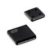
Package Type
PLCC
Mounting
Surface Mount
Pin Count
52
Lead Free Status / Rohs Status
Compliant
Available stocks
Company
Part Number
Manufacturer
Quantity
Price
Company:

Part Number:
SC68C562C1A
Manufacturer:
NXP
Quantity:
5 510
Company:
Part Number:
SC68C562C1A
Manufacturer:
ARK
Quantity:
5 510


Philips Semiconductors
PIN CONFIGURATION
PIN DESCRIPTION
2004 Mar 29
A1–A6
D0–D7
R/WN
CSN
IRQN
IACKN
X1/CLK
CMOS Dual universal serial communications controller
(CDUSCC)
MNEMONIC
33-30,
51-49
23-20
PIN
4-2,
28
27
47
6
1
TYPE
I/O
O
I
I
I
I
I
are enabled on D0–D7 as controlled by R/WN and A1–A6 inputs. When CSN is HIGH, the data lines
drive the internal bit rate generator, as an optional input to the counter/timer or DPLL, and to provide
Address Lines: Active-HIGH. Address inputs which specify which of the internal registers is
accessed for read/write operation.
Bidirectional Data Bus: Active-HIGH, 3-State. Bit 0 is the LSB and bit 7 is the MSB. All data,
command and status transfers between the CPU and the CDUSCC take place over this bus. The
data bus is enabled when CSN and R/WN or during interrupt acknowledge cycles and single
address DMA acknowledge cycles.
Read/Write: A HIGH input indicates a read cycle and a LOW indicates a write cycle when CEN is
active.
Chip Select: Active-LOW input. When active, data transfers between the CPU and the CDUSCC
are placed in the 3-State condition (except during interrupt acknowledge cycles and single address
DMA transfers).
Interrupt Request: Active-LOW, open-drain. This output is asserted upon occurrence of any
enabled interrupting condition. The CPU can read the general status register to determine the
interrupting condition(s), or can respond with an interrupt acknowledge cycle to cause the CDUSCC
to output an interrupt vector on the data bus.
Interrupt Acknowledge: Active-LOW. When IACKN is asserted, the CDUSCC responds by either
forcing the bus into high-impedance, placing a vector number, call instruction or zero on the data
bus. The vector number can be modified or unmodified by the status. If no interrupt is pending,
IACKN is ignored and the data bus placed in high-impedance.
Crystal or External Clock: When using the crystal oscillator, the crystal is connected between pins
X1 and X2. If a crystal is not used, an external clock is supplied at this input. This clock is used to
other required clocking signals. When a crystal is used, a capacitor must be connected from this pin
to ground.
CORNER
Pin Function
6
8
10 TRxCB
11 RTxCB
12 DCDBN/SYNIBN
13 NC
14 RxDB
15 TxDB
16 TxDAKBN/GPI2BN
17 RTxDRQBN/GPO1BN
18 TxDRQBN/GPO2BN/RTSBN
19 CTSBN/LCBN
20 D7
21 D6
22 D5
23 D4
24 DTACKN
25 DTCN
26 GND
1
2
3
4
5
7
9 RTSBN/SYNOUTBN
INDEX
IACKN
A3
A2
A1
RTxDAKBN/GPI1BN
IRQN
NC
RESETN
20
8
21
7
TOP VIEW
PLCC
1
5
47
33
Pin Function
27 CSN
28 R/WN
29 DONEN
30 D3
31 D2
32 D1
33 D0
34 NC
35 CTSAN/LCAN
36 TxDRQAN/GPO2AN/RTSAN
37 RTxDRQAN/GPO1AN
38 TxDAKAN/GPI2AN
39 TxDA
40 RxDA
41 NC
42 DCDAN/SYNIAN
43 RTxCA
44 TRxCA
45 RTSAN/SYNOUTAN
46 X2/IDCN
47 X1/CLK
48 RTxDAKAN/GPI1AN
49 A6
50 A5
51 A4
52 V
NAME AND FUNCTION
46
34
DD
SD00739
SC68C562
Product data
Related parts for SC68C562C1A
Image
Part Number
Description
Manufacturer
Datasheet
Request
R

Part Number:
Description:
NXP Semiconductors designed the LPC2420/2460 microcontroller around a 16-bit/32-bitARM7TDMI-S CPU core with real-time debug interfaces that include both JTAG andembedded trace
Manufacturer:
NXP Semiconductors
Datasheet:

Part Number:
Description:
NXP Semiconductors designed the LPC2458 microcontroller around a 16-bit/32-bitARM7TDMI-S CPU core with real-time debug interfaces that include both JTAG andembedded trace
Manufacturer:
NXP Semiconductors
Datasheet:
Part Number:
Description:
NXP Semiconductors designed the LPC2468 microcontroller around a 16-bit/32-bitARM7TDMI-S CPU core with real-time debug interfaces that include both JTAG andembedded trace
Manufacturer:
NXP Semiconductors
Datasheet:
Part Number:
Description:
NXP Semiconductors designed the LPC2470 microcontroller, powered by theARM7TDMI-S core, to be a highly integrated microcontroller for a wide range ofapplications that require advanced communications and high quality graphic displays
Manufacturer:
NXP Semiconductors
Datasheet:
Part Number:
Description:
NXP Semiconductors designed the LPC2478 microcontroller, powered by theARM7TDMI-S core, to be a highly integrated microcontroller for a wide range ofapplications that require advanced communications and high quality graphic displays
Manufacturer:
NXP Semiconductors
Datasheet:
Part Number:
Description:
The Philips Semiconductors XA (eXtended Architecture) family of 16-bit single-chip microcontrollers is powerful enough to easily handle the requirements of high performance embedded applications, yet inexpensive enough to compete in the market for hi
Manufacturer:
NXP Semiconductors
Datasheet:
Part Number:
Description:
The XA-S3 device is a member of Philips Semiconductors? XA(eXtended Architecture) family of high performance 16-bitsingle-chip microcontrollers
Manufacturer:
NXP Semiconductors
Datasheet:

Part Number:
Description:
The NXP BlueStreak LH75401/LH75411 family consists of two low-cost 16/32-bit System-on-Chip (SoC) devices
Manufacturer:
NXP Semiconductors
Datasheet:
Part Number:
Description:
The NXP LPC3130/3131 combine an 180 MHz ARM926EJ-S CPU core, high-speed USB2
Manufacturer:
NXP Semiconductors
Datasheet:
Part Number:
Description:
The NXP LPC3141 combine a 270 MHz ARM926EJ-S CPU core, High-speed USB 2
Manufacturer:
NXP Semiconductors
Part Number:
Description:
The NXP LPC3143 combine a 270 MHz ARM926EJ-S CPU core, High-speed USB 2
Manufacturer:
NXP Semiconductors

Part Number:
Description:
The NXP LPC3152 combines an 180 MHz ARM926EJ-S CPU core, High-speed USB 2
Manufacturer:
NXP Semiconductors
Part Number:
Description:
The NXP LPC3154 combines an 180 MHz ARM926EJ-S CPU core, High-speed USB 2
Manufacturer:
NXP Semiconductors

Part Number:
Description:
Standard level N-channel enhancement mode Field-Effect Transistor (FET) in a plastic package using NXP High-Performance Automotive (HPA) TrenchMOS technology
Manufacturer:
NXP Semiconductors
Datasheet: