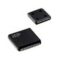
SC68C562C1A NXP Semiconductors, SC68C562C1A Datasheet - Page 2

SC68C562C1A
Manufacturer Part Number
SC68C562C1A
Description
Manufacturer
NXP Semiconductors
Datasheet
1.SC68C562C1A.pdf
(24 pages)
Specifications of SC68C562C1A
Operating Supply Voltage (typ)
5V
Operating Temp Range
0C to 70C
Operating Temperature Classification
Commercial
Package Type
PLCC
Mounting
Surface Mount
Pin Count
52
Lead Free Status / Rohs Status
Compliant
Available stocks
Company
Part Number
Manufacturer
Quantity
Price
Company:
Part Number:
SC68C562C1A
Manufacturer:
NXP
Quantity:
5 510
Company:
Part Number:
SC68C562C1A
Manufacturer:
ARK
Quantity:
5 510
phase-locked loop (DPLL), a parity/CRC generator and checker, and
rate generator (BRG), operating directly from a crystal or an external
Philips Semiconductors
DESCRIPTION
The Philips Semiconductors SC68C562 Dual Universal Serial
Communications Controller (CDUSCC) is a single-chip CMOS-LSI
communications device that provides two independent,
multi-protocol, full-duplex receiver/transmitter channels in a single
package. It supports bit-oriented and character-oriented (byte count
and byte control) synchronous data link controls as well as
asynchronous protocols. The SC68C562 interfaces to the 68000
MPUs via asynchronous bus control signals and is capable of
program-polled, interrupt driven, block-move or DMA data transfers.
The SC68C562 is hardware (pin) and software (Register)
compatible with SCN68562 (NMOS version). It will automatically
configure to NMOS DUSCC register map on power-up or reset.
The operating mode and data format of each channel can be
programmed independently. Each channel consists of a receiver, a
transmitter, a 16-bit multifunction counter/timer, a digital
associated control circuits. The two channels share a common bit
clock, which provides 16 common bit rates simultaneously. The
operating rate for the receiver and transmitter of each channel can
be independently selected from the BRG, the DPLL, the
counter/timer, or from an external 1X or 16X clock.
This makes the CDUSCC well suited for dual speed channel
applications. Data rates up to 10 Mb/s are supported.
Each transmitter and each receiver is serviced by a 16-byte FIFO.
The receiver FIFO also stores 9 status bits for each character
received; the transmit FIFO is able to store transmitter commands
with each byte. This permits reading and writing of up to 16 bytes at
a time, thus minimizing the potential for transmitter underrun,
receiver overrun and reducing interrupt or DMA overhead.
In addition, a flow control capability is provided to disable a remote
transmitter when the FIFO of the local receiving device is full. Two
modem control inputs (DCD and CTS) and three modem control
outputs (RTS and two general purpose) are provided. Because the
modem control inputs are general purpose in nature, they can be
optionally programmed for other functions. This document contains
the electrical specifications for the SC68C562. Refer to the CMOS
Dual Universal Serial Communications Controller (CDUSCC) User
Manual for a complete operational description of this product.
FEATURES
General Features
2004 Mar 29
– BOP: HDLC/ADCCP, SDLC, SDLC loop, X.25 or X.75 link level,
Full hardware and software upward compatibility with previous
NMOS device
Dual full-duplex synchronous/ asynchronous receiver and
transmitter
Low power CMOS process
Multiprotocol operation
– COP: BISYNC, DDCMP
– ASYNC: 5–8 bits plus optional parity
Sixteen character receiver and transmitter FIFOs
0 to 10 MHz data rate
CMOS Dual universal serial communications controller
(CDUSCC)
etc.
2
Asynchronous Mode Features
Programmable bit rate for each receiver and transmitter selectable
from:
– 19 fixed rates: 50 to 64 kbaud
– One user-defined rate derived from programmable
– External 1X or 16X clock
– Digital phase-locked loop
Parity and FCS (frame check sequence LRC or CRC) generation
and checking
Programmable data encoding/decoding: NRZ, NRZI, FM0, FM1,
Manchester
Programmable channel mode: full- and half-duplex, auto-echo, or
local loopback
Programmable data transfer mode: polled, interrupt, DMA, wait
DMA interface
– Compatible with the Philips Semiconductors SCB68430 Direct
– Single- or dual-address dual transfers
– Half- or full-duplex operation
– Automatic frame termination on counter/timer terminal count or
Transmit path clear status
Interrupt capabilities
– Daisy chain option
– Vector output (fixed or modified by status)
– Programmable internal priorities
– Interrupt at any FIFO fill level
– Maskable interrupt conditions
FIFO’d status bits
Watchdog timer
Multi-function programmable 16-bit counter/timer
– Bit rate generator
– Event counter
– Count received or transmitted characters
– Delay generator
– Automatic bit length measurement
Modem controls
– RTS, CTS, DCD, and up to four general I/O pins per channel
– CTS and DCD programmable auto-enables for Tx and Rx
– Programmable interrupt on change of CTS or DCD
On-chip oscillator for crystal
TTL compatible
Single +5 V power supply
Character length: 5 to 8 bits
Odd or even parity, no parity, or force parity
Up to two stop bits programmable in 1/16-bit increments
1X or 16X Rx and Tx clock factors
counter/timer
Memory Access Interface (DMAI) and other DMA controllers
DMA DONE
SC68C562
Product data


