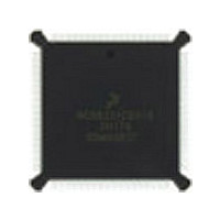
DSP56002FC66 Freescale Semiconductor, DSP56002FC66 Datasheet - Page 20

DSP56002FC66
Manufacturer Part Number
DSP56002FC66
Description
Manufacturer
Freescale Semiconductor
Datasheet
1.DSP56002FC66.pdf
(110 pages)
Specifications of DSP56002FC66
Device Core Size
24b
Architecture
Harvard
Format
Fixed Point
Clock Freq (max)
66MHz
Mips
33
Device Input Clock Speed
66MHz
Ram Size
3KB
Program Memory Size
1.5KB
Operating Supply Voltage (typ)
5V
Operating Supply Voltage (min)
4.5V
Operating Supply Voltage (max)
5.5V
Operating Temp Range
-40C to 105C
Operating Temperature Classification
Industrial
Mounting
Surface Mount
Pin Count
132
Package Type
PQFP
Lead Free Status / Rohs Status
Supplier Unconfirmed
Available stocks
Company
Part Number
Manufacturer
Quantity
Price
Company:
Part Number:
DSP56002FC66
Manufacturer:
MOTOROLA
Quantity:
5 530
Company:
Part Number:
DSP56002FC66
Manufacturer:
MOTOROLA
Quantity:
6 250
Company:
Part Number:
DSP56002FC66
Manufacturer:
MOTOROLA
Quantity:
591
Part Number:
DSP56002FC66
Manufacturer:
MOTOROLA/摩托罗拉
Quantity:
20 000
Company:
Part Number:
DSP56002FC661H72G
Manufacturer:
AD
Quantity:
92
Signal/Pin Descriptions
Serial Communications Interface Port
1-14
SERIAL COMMUNICATIONS INTERFACE PORT
RXD
PC0
TXD
PC1
SCLK
PC2
Signal Name
Output
Output
Output
Output
Signal
Input
Input
Input
Input
Type
Table 1-10 Serial Communications Interface (SCI+) Signals
or
or
or
Tri-stated Receive Data (RXD)—This input receives byte-oriented data and
Tri-stated Transmit Data (TXD)—This output transmits serial data from
Tri-stated SCI Clock (SCLK)—This signal provides an input or output
during
Reset
State
Freescale Semiconductor, Inc.
For More Information On This Product,
transfers the data to the SCI receive shift register. Input data can be
sampled on either the positive edge or on the negative edge of the
receive clock, depending on how the SCI control register is
programmed.
Port C GPIO 0 (PC0)—This signal is a GPIO signal called PC0
when the SCI RXD function is not being used.
After reset, the default state is GPIO input.
the SCI transmit shift register. In the default configuration, the
data changes on the positive clock edge and is valid on the
negative clock edge. The user can reverse this clock polarity by
programming the SCI control register appropriately.
Port C GPIO 1 (PC1)—This signal is a GPIO signal called PC1
when the SCI TXD function is not being used.
After reset, the default state is GPIO input.
clock from which the receive or transmit baud rate is derived in
the Asynchronous mode, and from which data is transferred in
the Synchronous mode. The direction and function of the signal
is defined by the RCM bit in the SCI+ Clock Control Register
(SCCR).
Port C GPIO 2 (PC2)—This signal is a GPIO signal called PC2
when the SCI SCLK function is not being used.
After reset, the default state is GPIO input.
DSP56002/D, Rev. 3
Go to: www.freescale.com
Signal Description
MOTOROLA


