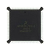
DSP56002FC66 Freescale Semiconductor, DSP56002FC66 Datasheet - Page 14

DSP56002FC66
Manufacturer Part Number
DSP56002FC66
Description
Manufacturer
Freescale Semiconductor
Datasheet
1.DSP56002FC66.pdf
(110 pages)
Specifications of DSP56002FC66
Device Core Size
24b
Architecture
Harvard
Format
Fixed Point
Clock Freq (max)
66MHz
Mips
33
Device Input Clock Speed
66MHz
Ram Size
3KB
Program Memory Size
1.5KB
Operating Supply Voltage (typ)
5V
Operating Supply Voltage (min)
4.5V
Operating Supply Voltage (max)
5.5V
Operating Temp Range
-40C to 105C
Operating Temperature Classification
Industrial
Mounting
Surface Mount
Pin Count
132
Package Type
PQFP
Lead Free Status / Rohs Status
Supplier Unconfirmed
Available stocks
Company
Part Number
Manufacturer
Quantity
Price
Company:
Part Number:
DSP56002FC66
Manufacturer:
MOTOROLA
Quantity:
5 530
Company:
Part Number:
DSP56002FC66
Manufacturer:
MOTOROLA
Quantity:
6 250
Company:
Part Number:
DSP56002FC66
Manufacturer:
MOTOROLA
Quantity:
591
Part Number:
DSP56002FC66
Manufacturer:
MOTOROLA/摩托罗拉
Quantity:
20 000
Company:
Part Number:
DSP56002FC661H72G
Manufacturer:
AD
Quantity:
92
Signal/Pin Descriptions
Bus Control
BUS CONTROL
1-8
PS
DS
X/Y
BS
BR
BG
Signal
Name
Output Tri-stated Program Memory Select—PS is asserted low for external program
Output Tri-stated Data Memory Select—DS is asserted low for external data memory
Output Tri-stated X/Y External Memory Select—This output is driven low during
Output Pulled
Output Pulled
Signal
Type
Input
high
Input
high
during
Reset
State
Freescale Semiconductor, Inc.
memory access. PS is tri-stated when the BG or RESET signal is
asserted.
access. DS is tri-stated when the BG or RESET signal is asserted.
external Y data memory accesses. It is also driven low during external
exception vector fetches when operating in the Development mode.
X/Y is tri-stated when the BG or RESET signal is asserted.
Bus Select—BS is asserted when the DSP accesses the external bus,
and it acts as an early indication of imminent external bus access by
the DSP56002. It may also be used with the bus wait input WT to
generate wait states. BS is pulled high when the BG or RESET signal is
asserted.
Bus Request—When the Bus Request input (BR) is asserted, it allows
an external device, such as another processor or DMA controller, to
become the master of the external address and data buses. While the
bus is released, the DSP may continue internal operations using
internal memory spaces. When BR is deasserted, the DSP56002 is the
bus master.When BR is asserted, the DSP56002 will release Port A,
including A0–A15, D0–D23, and the bus control signals (PS, DS, X/Y,
RD, WR, and BS) by placing them in the high-impedance state after
execution of the current instruction has been completed.
Note:
Bus Grant—When this output is asserted, it grants an external
device’s request for access to the external bus. This output is
deasserted during hardware reset.
For More Information On This Product,
Table 1-7 Bus Control Signals
DSP56002/D, Rev. 3
To prevent erroneous operation, pull up the BR signal when it
is not in use.
Go to: www.freescale.com
Signal Description
MOTOROLA


