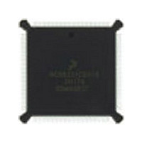
DSP56002FC66 Freescale Semiconductor, DSP56002FC66 Datasheet - Page 18

DSP56002FC66
Manufacturer Part Number
DSP56002FC66
Description
Manufacturer
Freescale Semiconductor
Datasheet
1.DSP56002FC66.pdf
(110 pages)
Specifications of DSP56002FC66
Device Core Size
24b
Architecture
Harvard
Format
Fixed Point
Clock Freq (max)
66MHz
Mips
33
Device Input Clock Speed
66MHz
Ram Size
3KB
Program Memory Size
1.5KB
Operating Supply Voltage (typ)
5V
Operating Supply Voltage (min)
4.5V
Operating Supply Voltage (max)
5.5V
Operating Temp Range
-40C to 105C
Operating Temperature Classification
Industrial
Mounting
Surface Mount
Pin Count
132
Package Type
PQFP
Lead Free Status / Rohs Status
Supplier Unconfirmed
Available stocks
Company
Part Number
Manufacturer
Quantity
Price
Company:
Part Number:
DSP56002FC66
Manufacturer:
MOTOROLA
Quantity:
5 530
Company:
Part Number:
DSP56002FC66
Manufacturer:
MOTOROLA
Quantity:
6 250
Company:
Part Number:
DSP56002FC66
Manufacturer:
MOTOROLA
Quantity:
591
Part Number:
DSP56002FC66
Manufacturer:
MOTOROLA/摩托罗拉
Quantity:
20 000
Company:
Part Number:
DSP56002FC661H72G
Manufacturer:
AD
Quantity:
92
Signal/Pin Descriptions
Host Interface (HI) Port
HOST INTERFACE (HI) PORT
1-12
H0–H7
PB0–PB7
HA0–HA2
PB8–PB10
HR/W
PB11
Signal
Name
Output
Output
Output
Signal
Input
Input
Input
Input
Input
Type
or
or
or
Tri-stated Host Data Bus (H0–H7)—This data bus transfers data between
Tri-stated Host Address 0—Host Address 2 (HA0–HA2)—These inputs
Tri-stated Host Read/Write—This input selects the direction of data
during
Reset
State
Freescale Semiconductor, Inc.
For More Information On This Product,
unless HR/W is high and HEN is asserted, in which case H0–H7
become outputs, allowing the host processor to read the
DSP56002 data. H0–H7 become outputs when HACK is asserted
during HREQ assertion.
transfer for each host processor access. If HR/W is high and HEN
inputs and host data is transferred to the DSP. HR/W must be
stable when HEN is asserted.
Port B GPIO 11 (PB11)—This signal is a General Purpose I/O
signal called PB11 when the Host Interface is not being used.
After reset, the default state for this signal is GPIO input.
the host processor and the DSP56002.
When configured as a Host Interface port, the H0–H7signals are
tri-stated as long as HEN is deasserted. The signals are inputs
Port B GPIO 0–7 (PB0–PB7)—These signals are General Purpose
I/O signals (PB0–PB7) when the Host Interface is not selected.
After reset, the default state for these signals is GPIO input.
provide the address selection for each Host Interface register.
Port B GPIO 8–10 (PB8–PB10)—These signals are General
Purpose I/O signals (PB8–PB10) when the Host Interface is not
selected.
After reset, the default state for these signals is GPIO input.
is asserted, H0–H7 are outputs and DSP data is transferred to the
host processor. If HR/W is low and HEN is asserted, H0–H7 are
DSP56002/D, Rev. 3
Table 1-9 HI Signals
Go to: www.freescale.com
Signal Description
MOTOROLA


