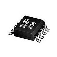
PHC21025 NXP Semiconductors, PHC21025 Datasheet - Page 3

PHC21025
Manufacturer Part Number
PHC21025
Description
Intermediate level N-channel and P-channel complementary pair enhancement mode Field-Effect Transistor (FET) in a plastic package using vertical D-MOS technology
Manufacturer
NXP Semiconductors
Type
Power MOSFETr
Datasheet
1.PHC21025.pdf
(16 pages)
Specifications of PHC21025
Number Of Elements
2
Polarity
N/P
Channel Mode
Enhancement
Drain-source On-volt
30V
Gate-source Voltage (max)
20V
Power Dissipation
2W
Operating Temp Range
-65C to 150C
Operating Temperature Classification
Military
Mounting
Surface Mount
Pin Count
8
Package Type
SO
Lead Free Status / Rohs Status
Compliant
Available stocks
Company
Part Number
Manufacturer
Quantity
Price
Company:
Part Number:
PHC21025
Manufacturer:
NXP
Quantity:
60 000
Part Number:
PHC21025
Manufacturer:
PHILIPS/飞利浦
Quantity:
20 000
NXP Semiconductors
4. Limiting values
Table 4.
In accordance with the Absolute Maximum Rating System (IEC 60134).
[1]
[2]
[3]
[4]
[5]
[6]
PHC21025
Product data sheet
Symbol
V
V
V
I
I
P
T
T
Source-drain diode
I
I
D
DM
S
SM
stg
j
DS
GS
GSO
tot
Pulse width and duty cycle limited by maximum junction temperature.
Maximum permissible dissipation per MOS transistor. Device mounted on printed-circuit board with a thermal resistance from ambient to
solder point of 90 K/W.
Maximum permissible dissipation per MOS transistor. Both devices may be loaded up to 2 W at the same time.
Maximum permissible dissipation if only one MOS transistor dissipates. Device mounted on printed-circuit board with thermal resistance
from ambient to solder point of 90 K/W.
Maximum permissible dissipation per MOS transistor. Device mounted on printed-circuit board with a Thermal resistance from ambient
to solder point of 27.5 K/W.
Pulse width and duty cycle limited by maximum junction temperature.
Limiting values
Parameter
drain-source voltage
gate-source voltage
gate-source voltage
drain current
peak drain current
total power dissipation
storage temperature
junction temperature
source current
peak source current
All information provided in this document is subject to legal disclaimers.
open drain
Conditions
T
T
T
T
T
see
T
see
T
T
T
T
T
T
T
Rev. 04 — 17 March 2011
j
j
sp
sp
sp
sp
amb
sp
amb
sp
sp
sp
sp
≥ 25 °C; T
≥ 25 °C; T
≤ 80 °C; P-channel
≤ 80 °C; N-channel
= 25 °C; pulsed; N-channel;
= 25 °C; pulsed; P-channel;
= 80 °C; see
≤ 80 °C; P-channel
≤ 80 °C; N-channel
= 25 °C; pulsed; P-channel
= 25 °C; pulsed; N-channel
Figure 2
Figure 3
= 25 °C
= 25 °C
j
j
≤ 150 °C; N-channel
≤ 150 °C; P-channel
Figure 1
Complementary intermediate level FET
[1]
[1]
[2]
[3]
[4]
[5]
[6]
[6]
PHC21025
Min
-
-
-
-20
-
-
-
-
-
-
-
-
-65
-
-
-
-
-
© NXP B.V. 2011. All rights reserved.
20
150
Max
30
-30
-
-2.3
3.5
14
-10
1
2
1.3
2
150
-1.25
1.5
-5
6
Unit
V
V
V
V
A
A
A
A
W
W
W
W
°C
°C
A
A
A
A
3 of 16


