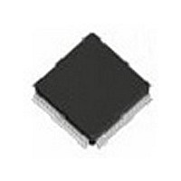
ADSP-2171KST-133 Analog Devices Inc, ADSP-2171KST-133 Datasheet - Page 7

ADSP-2171KST-133
Manufacturer Part Number
ADSP-2171KST-133
Description
Manufacturer
Analog Devices Inc
Datasheet
1.ADSP-2171KST-133.pdf
(52 pages)
Specifications of ADSP-2171KST-133
Device Core Size
16b
Architecture
Enhanced Harvard
Format
Fixed Point
Clock Freq (max)
33.33MHz
Mips
33
Device Input Clock Speed
33.33MHz
Ram Size
10KB
Program Memory Size
24KB
Operating Supply Voltage (typ)
5V
Operating Supply Voltage (min)
4.5V
Operating Supply Voltage (max)
5.5V
Operating Temp Range
0C to 70C
Operating Temperature Classification
Commercial
Mounting
Surface Mount
Pin Count
128
Package Type
TQFP
Lead Free Status / Rohs Status
Not Compliant
REV. A
Because the ADSP-217x includes an on-chip oscillator circuit,
an external crystal may be used. The crystal should be con-
nected across the CLKIN and XTAL pins, with two capacitors
connected as shown in Figure 4. A parallel-resonant, fundamen-
tal frequency, microprocessor-grade crystal should be used.
A clock output (CLKOUT) signal is generated by the processor
at the processor’s cycle rate. This can be enabled and disabled
by the CLKODIS bit in the SPORT0 Autobuffer Control Reg-
ister, DM[0x3FF3].
Reset
The RESET signal initiates a master reset of the ADSP-217x.
The RESET signal must be asserted during the power-up se-
quence to assure proper initialization. RESET during initial
power-up must be held long enough to allow the internal clock
Figure 4. External Crystal Connections
3
A
CLKOUT
RESET
IRQ2
BR
BG
FL2-0
MMAP
NOTE:
THE TWO MSBs OF THE DATA BUS ARE USED AS THE MSBs OF THE BOOT EPROM ADDRESS.
THIS IS ONLY REQUIRED FOR THE 27C256 AND 27C512.
CLKIN
(OPTIONAL)
PROGRAM
MEMORY
CLOCK OR
CRYSTAL
24
CLKIN
ADSP-217x
D
XTAL
PMS
CS
XTAL
WE
OE
PWD
RD
CLKOUT
PWDACK
Figure 3. ADSP-217x Basic System Configuration
WR
ADSP-217x
6
V
ADDRESS
OE
WE
14
DD
A
DATA MEMORY
9
GND
PERIPHERALS
(OPTIONAL)
16
24
DATA
D
23-8
D
&
4
MODE
HOST
–7–
to stabilize. If RESET is activated any time after power-up, the
clock continues to run and does not require stabilization time.
The power-up sequence is defined as the total time required for
the crystal oscillator circuit to stabilize after a valid V
plied to the processor, and for the internal phase-locked loop
(PLL) to lock onto the specific crystal frequency. A minimum of
2000 CLKIN cycles ensures that the PLL has locked but does
not include the crystal oscillator start-up time. During this
power-up sequence the RESET signal should be held low. On
any subsequent resets, the RESET signal must meet the mini-
mum pulse width specification, t
The RESET input contains some hysteresis; however, if you use
an RC circuit to generate your RESET signal, the use of an ex-
ternal Schmidt trigger is recommended.
The master reset sets all internal stack pointers to the empty
stack condition, masks all interrupts and clears the MSTAT reg-
ister. When RESET is released, if there is no pending bus re-
quest and the chip is configured for booting (MMAP = 0), the
boot-loading sequence is performed. Then the first instruction is
fetched from internal program memory location 0x0000.
DMS
CS
7
ADSP-2171/ADSP-2172/ADSP-2173
SERIAL
PORT 0
SERIAL
PORT 1
16
BMS
HIP
HIP CONTROL
HIP DATA/ADDR
OE
14
RFS
DR
SCLK
RFS or IRQ0
DT or FO
DR or FI
SCLK
TFS
DT
TFS or IRQ1
A
D
2
23-22
BOOT MEMORY
e.g., EPROM
27C128
27C256
27C512
27C64
RSP
D
8
15-8
D
.
SERIAL DEVICE
SERIAL DEVICE
PROCESSOR
(OPTIONAL)
(OPTIONAL)
(OPTIONAL)
CS
HOST
DD
is ap-


