FDS6690 Fairchild Semiconductor, FDS6690 Datasheet
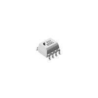
MOSFET Power USE 512-FDS6690A

FDS6690

Manufacturer Part Number
FDS6690
Description
MOSFET Power USE 512-FDS6690A
Manufacturer
Fairchild Semiconductor
Datasheet

Specifications of FDS6690

Configuration
Single Quad Drain Triple Source
Transistor Polarity
N-Channel
Resistance Drain-source Rds (on)
0.0125 Ohms
Forward Transconductance Gfs (max / Min)
48 S
Drain-source Breakdown Voltage
30 V
Gate-source Breakdown Voltage
+/- 20 V
Continuous Drain Current
11 A
Power Dissipation
2.5 W
Maximum Operating Temperature
+ 150 C
Mounting Style
SMD/SMT
Package / Case
SOIC-8 Narrow
Fall Time
10 ns
Minimum Operating Temperature
- 55 C
Rise Time
13 ns
Lead Free Status / Rohs Status
No

Available stocks

Company
Part Number
Manufacturer
Quantity
Price
Part Number:
FDS6690
Manufacturer:
FSC
Quantity:
50 000
Part Number:
FDS6690
Manufacturer:
FSC
Quantity:
296
Part Number:
FDS6690
Manufacturer:
FAIRCHILD/仙童
Quantity:
20 000
Part Number:
FDS6690-NL
Manufacturer:
FAIRCHILD/仙童
Quantity:
20 000
Part Number:
FDS6690A
Manufacturer:
NS
Quantity:
3
Part Number:
FDS6690A
Manufacturer:
FSC
Quantity:
38 400
Part Number:
FDS6690A
Manufacturer:
Fairchild Semiconductor
Quantity:
24 726
Part Number:
FDS6690A
Manufacturer:
FAIR
Quantity:
1 000
Part Number:
FDS6690A
Manufacturer:
FAIR
Quantity:
1 000
Part Number:
FDS6690A
Manufacturer:
FAIR
Quantity:
1 000
Part Number:
FDS6690A
Manufacturer:
FAIR
Quantity:
1 454
Part Number:
FDS6690A
Manufacturer:
FAIRCHILD
Quantity:
8 000
Part Number:
FDS6690A
Manufacturer:
FAIRCHILD/仙童
Quantity:
20 000
Part Number:
FDS6690A
0
Company:
Part Number:
FDS6690A
Quantity:
45 000
Company:
Part Number:
FDS6690A
Quantity:
10 000
Company:
Part Number:
FDS6690A
Quantity:
4 500
Symbol
V
V
I
P
T
THERMAL CHARACTERISTICS
R
R
© 1998 Fairchild Semiconductor Corporation
This N Channel Logic Level MOSFET has been designed
specifically to improve the overall efficiency of DC/DC
converters using either synchronous or conventional switching
PWM controllers.
The MOSFET features faster switching and lower gate charge
than other MOSFETs with comparable R
The result is a MOSFET that is easy and safer to drive (even at
very high frequencies), and DC/DC power supply designs with
higher overall efficiency.
D
FDS6690
Single N-Channel Logic Level PWM Optimized PowerTrench® MOSFET
Absolute Maximum Ratings
DSS
GSS
D
J
General Description
,T
JA
JC
STG
SOT-23
D
Parameter
Drain-Source Voltage
Gate-Source Voltage
Drain Current - Continuous
Power Dissipation for Single Operation
Operating and Storage Temperature Range
Thermal Resistance, Junction-to-Ambient
Thermal Resistance, Junction-to-Case
D
SO-8
D
D
- Pulsed
SuperSOT
pin 1
S
TM
-6
S
T
A
DS(ON)
= 25
S
o
specifications.
C unless other wise noted
G
SuperSOT
(Note 1a)
(Note 1b)
(Note 1c)
(Note 1)
(Note 1a)
(Note 1a)
TM
-8
Features
SO-8
10 A, 30 V. R
Optimized for use in switching DC/DC converters with
PWM controllers.
Very fast switching .
Low gate charge (Qg typ = 13 nC).
5
6
7
8
R
-55 to 150
FDS6690
DS(ON)
DS(ON)
±20
2.5
1.2
30
50
25
10
50
1
SOT-223
= 0.0135
= 0.0200
@ V
@ V
January 2000
GS
GS
= 10 V
= 4.5 V.
SOIC-16
2
1
3
4
FDS6690 Rev.C
Units
°C/W
°C/W
°C
W
V
V
A

Related parts for FDS6690

FDS6690 Summary of contents

Page 1

... Very fast switching . Low gate charge (Qg typ = 13 nC). TM SO-8 SuperSOT - unless other wise noted A (Note 1a) (Note 1a) (Note 1b) (Note 1c) (Note 1a) (Note 1) January 2000 = 0.0135 @ DS(ON 0.0200 @ V = 4.5 V. DS(ON) GS SOIC-16 SOT-223 FDS6690 30 ± 2.5 1.2 1 -55 to 150 50 25 FDS6690 Rev.C Units °C °C/W °C/W ...

Page 2

... GS GEN 2 105 C 0.02 in pad of 2oz copper. Min Typ Max 55°C J 100 -100 -4.5 0.011 0.0135 T =125°C 0.018 0.023 J 0.017 0. 1340 340 125 2.1 0.73 1.2 (Note 2) is guaranteed 125 C 0.003 in of 2oz copper. Units µA µ pad FDS6690 Rev.C ...

Page 3

... DRAIN CURRENT (A) D Drain Current and Gate Voltage 125° 25° GATE TO SOURCE VOLTAGE (V) GS Gate-to-Source Voltage 125°C A 25°C -55°C 0.2 0.4 0.6 0 BODY DIODE FORWARD VOLTAGE (V) SD Variation with Source Current and Temperature 1.4 FDS6690 Rev.C ...

Page 4

... Transient thermal response will change depending on the circuit board design. C iss C oss MHz rss 0 DRAIN TO SOURCE VOLTAGE (V) DS SINGLE PULSE R =125° C 25°C A 0.1 0 100 SINGLE PULSE TIME (SEC) Dissipation. R ( 125°C/W JA P(pk ( Duty Cycle 100 30 300 300 FDS6690 Rev.C ...

Page 5

SO-8 Tape and Reel Data and Package Dimensions SOIC(8lds) Packaging Configuration: Figure 1 SHI P OR STO RE N EAR ECT ROST ECT RO M AGN ETI ...

Page 6

... Dim A max 13" Diameter Option Reel Tape Size Dim A Dim B Option 7.00 0.059 12mm 7" Dia 177.8 1.5 13.00 0.059 12mm 13" Dia 330 1.5 1998 Fairchild Semiconductor Corporation User Direction of Feed Dimensions are in millimeter 1.55 1.60 1.75 10.25 5.50 8.0 +/-0 ...

Page 7

SO-8 Tape and Reel Data and Package Dimensions, continued SOIC-8 (FS PKG Code S1 Scale 1:1 on letter size paper Dimensions shown below are in: inches [millimeters] Part Weight per unit (gram): 0.0774 September 1998, Rev. ...

Page 8

... TRADEMARKS The following are registered and unregistered trademarks Fairchild Semiconductor owns or is authorized to use and is not intended exhaustive list of all such trademarks. ACEx™ CoolFET™ CROSSVOLT™ CMOS FACT™ FACT Quiet Series™ ® FAST FASTr™ GTO™ ...

Related keywords