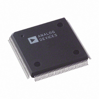
AD9887KS-140 Analog Devices Inc, AD9887KS-140 Datasheet - Page 36

AD9887KS-140
Manufacturer Part Number
AD9887KS-140
Description
IC INTRFACE ANALOG/DVI 160-MQFP
Manufacturer
Analog Devices Inc
Datasheet
1.AD9887AKSZ-100.pdf
(40 pages)
Specifications of AD9887KS-140
Rohs Status
RoHS non-compliant
Applications
Graphic Cards, VGA Interfaces
Interface
Analog and Digital
Voltage - Supply
3.15 V ~ 3.45 V
Package / Case
160-MQFP, 160-PQFP
Mounting Type
Surface Mount
Available stocks
Company
Part Number
Manufacturer
Quantity
Price
Company:
Part Number:
AD9887KS-140
Manufacturer:
ADI
Quantity:
440
Part Number:
AD9887KS-140
Manufacturer:
ADI/亚德诺
Quantity:
20 000
AD9887
1B
1C
1C
1C
2-WIRE SERIAL CONTROL PORT
A 2-wire serial interface control interface is provided. Up to four
AD9887 devices may be connected to the 2-wire serial interface,
with each device having a unique address.
The 2-wire serial interface comprises a clock (SCL) and a bidi-
rectional data (SDA) pin. The Analog Flat Panel Interface acts
as a slave for receiving and transmitting data over the serial
interface. When the serial interface is not active, the logic levels
on SCL and SDA are pulled HIGH by external pull-up resistors.
Data received or transmitted on the SDA line must be stable for
the duration of the positive-going SCL pulse. Data on SDA must
change only when SCL is LOW. If SDA changes state while SCL
is HIGH, the serial interface interprets that action as a start or
stop sequence.
There are five components to serial bus operation:
• Start Signal
• Slave Address Byte
• Base Register Address Byte
• Data Byte to Read or Write
• Stop Signal
When the serial interface is inactive (SCL and SDA are HIGH)
communications are initiated by sending a start signal. The start
signal is a HIGH-to-LOW transition on SDA while SCL is
HIGH. This signal alerts all slaved devices that a data transfer
sequence is coming.
The first eight bits of data transferred after a start signal comprising
a 7-bit slave address (the first seven bits) and a single R/W bit (the
7–0 Test Register
Must be set to 10H for proper operation.
7–2 Test Bits
Must be set to 6FH for proper operation.
1 Output Format Mode Select
A bit that configures the output data in 4:2:2 mode. This
mode can be used to reduce the number of data lines used
from 24 down to 16 for applications using YUV, YCbCr,
or YPbPr graphics signals. A timing diagram for this mode is
shown on page 22. Recommended input and output con-
figurations are shown in Table LI. In 4:2:2 mode, the red
and blue channels can be interchanged to help satisfy
board layout or timing requirements, but the green channel
must be configured for Y.
Select
1
1
Channel
Red
Green
Blue
1–0 Test Bits
Must be set to default.
Table LII. 4:2:2 Input/Output Configuration
Table LI. 4:2:2 Output Mode Select
U
Input
Connection
V
Y
Output Mode
4:4:4
4:2:2
Output
Format
U/V
Y
High Impedance
eighth bit). The R/W bit indicates the direction of data transfer,
read from (1) or write to (0) the slave device. If the transmitted
slave address matches the address of the device (set by the state of
the SA
bringing SDA LOW on the 9th SCL pulse. If the addresses do not
match, the AD9887 does not acknowledge.
Bit 7
A
(MSB)
1
1
1
1
Data Transfer via Serial Interface
For each byte of data read or written, the MSB is the first bit of
the sequence.
If the AD9887 does not acknowledge the master device during a
write sequence, the SDA remains HIGH so the master can
generate a stop signal. If the master device does not acknowledge
the AD9887 during a read sequence, the AD9887 interprets this
as “end of data.” The SDA remains HIGH so the master can
generate a stop signal.
Writing data to specific control registers of the AD9887 requires
that the 8-bit address of the control register of interest be written
after the slave address has been established. This control register
address is the base address for subsequent write operations. The
base address autoincrements by one for each byte of data written
after the data byte intended for the base address. If more bytes
are transferred than there are available addresses, the address will
not increment and remain at its maximum value of 1Dh. Any base
address higher than 1Dh will not produce an acknowledge signal.
Data is read from the control registers of the AD9887 in a similar
manner. Reading requires two data transfer operations:
The base address must be written with the R/W bit of the slave
address byte LOW to set up a sequential read operation.
Reading (the R/W bit of the slave address byte HIGH) begins at
the previously established base address. The address of the read
register autoincrements after each byte is transferred.
To terminate a read/write sequence to the AD9887, a stop sig-
nal must be sent. A stop signal comprises a LOW-to-HIGH
transition of SDA while SCL is HIGH.
A repeated start signal occurs when the master device driving
the serial interface generates a start signal without first generat-
ing a stop signal to terminate the current communication. This
is used to change the mode of communication (read, write)
between the slave and master without releasing the serial inter-
face lines.
Serial Interface Read/Write Examples
Write to one control register
6
➥Start signal
➥Slave Address byte (R/W bit = LOW)
➥Base Address byte
➥Data byte to base address
➥Stop signal
1-0
input pins in Table LIII, the AD9887 acknowledges by
Bit 6
A
0
0
0
0
5
Table LIII. Serial Port Addresses
Bit 5
A
0
0
0
0
4
Bit 4
A
1
1
1
1
3
Bit 3
A
1
1
1
1
2
Bit 2
A
0
0
1
1
1
Bit 1
A
0
1
0
1
0


