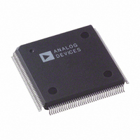
AD9887KS-140 Analog Devices Inc, AD9887KS-140 Datasheet - Page 14

AD9887KS-140
Manufacturer Part Number
AD9887KS-140
Description
IC INTRFACE ANALOG/DVI 160-MQFP
Manufacturer
Analog Devices Inc
Datasheet
1.AD9887AKSZ-100.pdf
(40 pages)
Specifications of AD9887KS-140
Rohs Status
RoHS non-compliant
Applications
Graphic Cards, VGA Interfaces
Interface
Analog and Digital
Voltage - Supply
3.15 V ~ 3.45 V
Package / Case
160-MQFP, 160-PQFP
Mounting Type
Surface Mount
Available stocks
Company
Part Number
Manufacturer
Quantity
Price
Company:
Part Number:
AD9887KS-140
Manufacturer:
ADI
Quantity:
440
Part Number:
AD9887KS-140
Manufacturer:
ADI/亚德诺
Quantity:
20 000
AD9887
clamping on the tip of HSYNC. Fortunately, there is virtually
always a period following HSYNC called the back porch where
a good black reference is provided. This is the time when clamp-
ing should be done.
The clamp timing can be established by exercising the CLAMP
pin at the appropriate time (with EXTCLMP = 1). The polarity
of this signal is set by the Clamp Polarity bit.
An easier method of clamp timing employs the AD9887 internal
clamp timing generator. The Clamp Placement register is pro-
grammed with the number of pixel clocks that should pass after
the trailing edge of HSYNC before clamping starts. A second
register (Clamp Duration) sets the duration of the clamp.
These are both 8-bit values, providing considerable flexibility in
clamp generation. The clamp timing is referenced to the trailing
edge of HSYNC, the back porch (black reference) always follows
HSYNC. A good starting point for establishing clamping is to
set the clamp placement to 08h (providing eight pixel periods
for the graphics signal to stabilize after sync) and set the clamp
duration to 14h (giving the clamp 20 pixel periods to reestablish
the black reference).
The value of the external input coupling capacitor affects the per-
formance of the clamp. If the value is too small, there can be an
amplitude change during a horizontal line time (between clamping
intervals). If the capacitor is too large, it will take excessively long for
the clamp to recover from a large change in incoming signal offset.
The recommended value (47 nF) results in recovery from a step error
of 100 mV to within 1/2 LSB in 10 lines using a clamp duration of
20 pixel periods on a 60 Hz SXGA signal.
YUV Clamping
YUV signals are slightly different from RGB signals in that the
dc reference level (black level in RGB signals) will be at the
midpoint of the U and V video signal. For these signals it can
be necessary to clamp to the midscale range of the A/D con-
verter range (80h) rather than bottom of the A/D converter
range (00h).
Clamping to midscale rather than ground can be accomplished
by setting the clamp select bits in the serial bus register. Each of
the three converters has its own selection bit so that they can be
clamped to either midscale or ground independently. These bits
are located in Register 0Fh and are Bits 0–2.
The midscale reference voltage that each A/D converter clamps
to is provided independently on the R
B
ence because both offset adjustment and gain adjustment for
each converter will affect the dc level of midscale.
During clamping, the Y and V converters are clamped to their
respective midscale reference input. These inputs are pins
B
The typical connections for both RGB and YUV clamping are
shown below in Figure 2. Note: if midscale clamping is not
required, all of the midscale voltage outputs should still be con-
nected to ground through a 0.1 µF capacitor.
MIDSC
CLAMP
V pins. Each converter must have its own midscale refer-
V, and R
CLAMP
V for the U and V converters respectively.
MIDSC
V, G
MIDSC
V, and
Gain and Offset Control
The AD9887 can accommodate input signals with inputs rang-
ing from 0.5 V to 1.0 V full scale. The full-scale range is set in
three 8-bit registers (Red Gain, Green Gain, and Blue Gain).
A code of 0 establishes a minimum input range of 0.5 V; 255
corresponds with the maximum range of 1.0 V. Note that
increasing the gain setting results in an image with less contrast.
The offset control shifts the entire input range, resulting in a
change in image brightness. Three 7-bit registers (Red Offset,
Green Offset, Blue Offset) provide independent settings for
each channel.
The offset controls provide a ± 63 LSB adjustment range. This
range is connected with the full-scale range, so if the input range
is doubled (from 0.5 V to 1.0 V) then the offset step size is also
doubled (from 2 mV per step to 4 mV per step).
Figure 3 illustrates the interaction of gain and offset controls.
The magnitude of an LSB in offset adjustment is proportional
to the full-scale range, so changing the full-scale range also
changes the offset. The change is minimal if the offset setting is
near midscale. When changing the offset, the full-scale range is
not affected, but the full-scale level is shifted by the same amount
as the zero-scale level.
1.0
0.5
0.0
00h
0.1 F
0.1 F
0.1 F
GAIN
R
R
G
G
B
B
MIDSC
CLAMP
MIDSC
CLAMP
MIDSC
CLAMP
OFFSET = 7Fh
V
V
V
V
V
V
OFFSET = 3Fh
OFFSET = 00h
OFFSET = 7Fh
OFFSET = 3Fh
OFFSET = 00h
FFh


