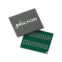
MT46H8M32LFB5-6:H Micron Technology Inc, MT46H8M32LFB5-6:H Datasheet - Page 70

MT46H8M32LFB5-6:H
Manufacturer Part Number
MT46H8M32LFB5-6:H
Description
IC SDRAM 256MB 166MHZ 90VFBGA
Manufacturer
Micron Technology Inc
Series
-r
Type
DDR SDRAMr
Specifications of MT46H8M32LFB5-6:H
Format - Memory
RAM
Memory Type
Mobile DDR SDRAM
Memory Size
256M (8Mx32)
Speed
166MHz
Interface
Parallel
Voltage - Supply
1.7 V ~ 1.95 V
Operating Temperature
0°C ~ 70°C
Package / Case
90-VFBGA
Organization
8Mx32
Density
256Mb
Address Bus
14b
Access Time (max)
6.5/5ns
Maximum Clock Rate
166MHz
Operating Supply Voltage (typ)
1.8V
Package Type
VFBGA
Operating Temp Range
0C to 70C
Operating Supply Voltage (max)
1.95V
Operating Supply Voltage (min)
1.7V
Supply Current
120mA
Pin Count
90
Mounting
Surface Mount
Operating Temperature Classification
Commercial
Lead Free Status / Rohs Status
Lead free / RoHS Compliant
Available stocks
Company
Part Number
Manufacturer
Quantity
Price
Company:
Part Number:
MT46H8M32LFB5-6:H
Manufacturer:
ST
Quantity:
34 600
Company:
Part Number:
MT46H8M32LFB5-6:H
Manufacturer:
Micron Technology Inc
Quantity:
10 000
Figure 32: Data Input Timing
PDF: 09005aef834bf85b
256mb_mobile_ddr_sdram_t36n.pdf - Rev. I 09/10 EN
Notes:
Data for any WRITE burst can be truncated by a subsequent PRECHARGE command, as
shown in Figure 42 (page 79) and Figure 43 (page 80). Note that only the data-in
pairs that are registered prior to the
any subsequent data-in should be masked with DM, as shown in Figure 42 (page 79)
and Figure 43 (page 80). After the PRECHARGE command, a subsequent command to
the same bank cannot be issued until
DQS
DM
CK#
DQ
CK
1. WRITE command issued at T0.
2.
3.
4. For x16, LDQS controls the lower byte; UDQS controls the upper byte. For x32, DQS0 con-
5. For x16, LDM controls the lower byte; UDM controls the upper byte. For x32, DM0 con-
4
5
t
t
trols DQ[7:0], DQS1 controls DQ[15:8], DQS2 controls DQ[23:16], and DQS3 controls
DQ[31:24].
trols DQ[7:0], DM1 controls DQ[15:8], DM2 controls DQ[23:16], and DM3 controls
DQ[31:24].
DSH (MIN) generally occurs during
DSS (MIN) generally occurs during
t
WPRES
T0
t
1
DQSS
t DS
T1
D
b
IN
t
WPRE
t
DSH
t DH
70
T1n
2
t
Transitioning Data
t
DQSL
DSS
256Mb: x16, x32 Mobile LPDDR SDRAM
t
WR period are written to the internal array, and
3
t
T2
t
RP is met.
t
DQSS (MAX).
DQSS (MIN).
Micron Technology, Inc. reserves the right to change products or specifications without notice.
t
t
DQSH
DSH
T2n
2
t
t
WPST
DSS
3
T3
Don’t Care
© 2008 Micron Technology, Inc. All rights reserved.
WRITE Operation


